Back contact solar cell with various tunnel junction structures and preparation method thereof

A technology of solar cells and tunnel junctions, applied in the field of solar cells, can solve the problems of efficiency loss, contact deterioration, metal area recombination surge, etc., to achieve high conversion efficiency, reduce process steps, and reduce the number of masks.

Pending Publication Date: 2020-02-25
TAIZHOU ZHONGLAI PHOTOELECTRIC TECH CO LTD
View PDF0 Cites 11 Cited by
  • Summary
  • Abstract
  • Description
  • Claims
  • Application Information

AI Technical Summary

Problems solved by technology

In 2017, Feldmann et al. from the Fraunhofer Institute for Solar Energy Systems in Germany increased the conversion efficiency of solar cells with tunnel oxide layer passivation metal contact structures to 25.8%, and the grid lines on the front surface of the cells caused ~0.2% efficiency loss
[0006] In addition, the most commonly used metallization method in the industriali

Method used


Image

  • Back contact solar cell with various tunnel junction structures and preparation method thereof
  • Back contact solar cell with various tunnel junction structures and preparation method thereof
  • Back contact solar cell with various tunnel junction structures and preparation method thereof

Examples


preparation example Construction

[0063] A method for preparing a back-contact solar cell with multiple tunnel junction structures provided by the present invention comprises the following steps:

[0064] (1) A tunnel oxide layer is grown on the back surface of the N-type crystalline silicon substrate, and an intrinsic polysilicon layer is deposited on the tunnel oxide layer to form c-Si / SiO X / i-poly tunnel junction; deposit an oxide layer on the intrinsic polysilicon layer, and deposit an intrinsic polysilicon layer on the oxide layer to form an i-poly / Oxide / i-poly tunnel junction;

[0065] (2) Deposit a mask on the n+ doped region of the front surface; then perform phosphorus doping on the intrinsic polysilicon layer, and activate or advance phosphorus atoms at high temperature, so that the intrinsic polysilicon layer is transformed into phosphorus-doped Polysilicon layer, forming c-Si / SiO X / n+poly tunnel junction and n+poly / Oxide / n+poly tunnel junction, while forming a phosphorus-containing silicon oxide...

Embodiment 1

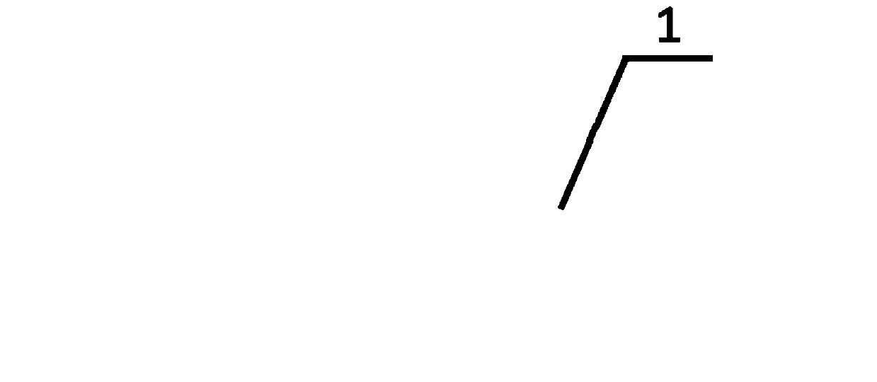
[0110] (1) Clean the front surface and the back surface of the N-type crystalline silicon substrate 1 respectively, remove the damaged layer and make texture, such as figure 1 Shown; Among them, the resistivity of the N-type silicon substrate is 0.3-10Ω·cm, and the thickness is 90-300μm.

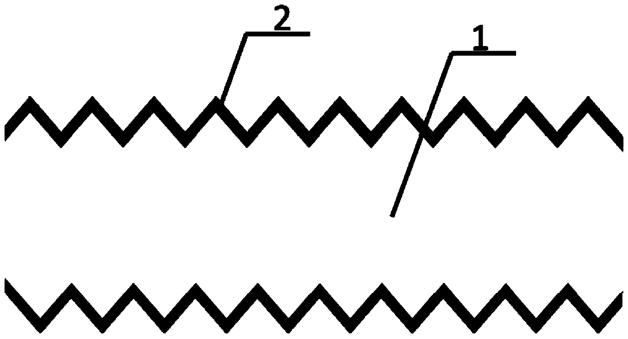
[0111] (2) Perform double-sided phosphorus diffusion on the N-type crystalline silicon substrate 1 after texturing to form a double-sided n+ doped region 2, such as figure 2 As shown; the phosphorus source is phosphorus oxychloride, the diffusion temperature is 800-1000°C, and the sheet resistance of the n+ doped region after phosphorus diffusion is 150-400Ω / sq.

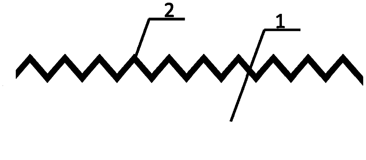
[0112] (3) etch the back surface of the N-type crystalline silicon substrate 1 and polish it, such as image 3 As shown; using heated TMAH or NaOH solution, the back n+ doped region 2 is removed and polished, and the weight loss of the silicon wafer is 0.1-0.5g.

[0113](4) grow an ultra-thin tunneling silicon dioxide layer 3 wi...

Embodiment 2

[0124] (1) Clean the front surface and the back surface of the N-type crystalline silicon substrate 1 respectively, remove the damaged layer and make texture, such as figure 1 Shown; Among them, the resistivity of the N-type silicon substrate is 0.3-10Ω·cm, and the thickness is 90-300μm.

[0125] (2) Perform double-sided phosphorus diffusion on the N-type crystalline silicon substrate 1 after texturing to form a double-sided n+ doped region 2, such as figure 2 As shown; the phosphorus source is phosphorus oxychloride, the diffusion temperature is 800-1000°C, and the sheet resistance of the n+ doped region after phosphorus diffusion is 150-400Ω / sq.

[0126] (3) etch the back surface of the N-type crystalline silicon substrate 1 and polish it, such as image 3 As shown; using heated TMAH or NaOH solution, the back n+ doped region 2 is removed and polished, and the weight loss of the silicon wafer is 0.1-0.5g.

[0127] (4) grow an ultra-thin tunneling silicon dioxide layer 3 w...


PUM

PropertyMeasurementUnit
Maximum widthaaaaaaaaaa
Depthaaaaaaaaaa
Thicknessaaaaaaaaaa

Abstract

The invention relates to a back contact solar cell with various tunnel junction structures and a preparation method thereof. The solar cell comprises an N-type crystalline silicon substrate; the frontsurface of the N-type crystalline silicon substrate comprises a lightly-doped n+ surface field and a passivation antireflection film, and the back surface of the N-type crystalline silicon substratecomprises a P-type emitter region, an N-type back surface field region and a groove structure; the P-type emitter region is located in the groove structure, and the N-type back surface field region islocated above the groove structure; the N-type back surface field region sequentially comprises a tunneling SiOX layer, an n+poly layer, an oxide layer, an n+poly layer, a tunneling SiOX layer and ap+poly layer from inside to outside; the SiOX layer and the n+poly layer form a c-Si/SiOX/n+poly tunnel junction; the oxide layer and the n+poly layer form an n+poly/Oxide/n+poly tunnel junction, andthe tunneling SiOX layer and the p+poly layer form an n+poly/SiOX/p+poly tunnel junction; the P-type emitter region sequentially comprises a tunneling SiOx layer and a p+poly layer from inside to outside, and the SiOx layer and the p+poly layer form a c-Si/SiOX/p+poly tunnel junction; the P-type emitter region is provided with a P-type metal electrode, and the N-type back surface field region is provided with an N-type metal electrode.

Description

technical field [0001] The invention relates to the technical field of solar cells, in particular to a back-contact solar cell with multiple tunnel junction structures and a preparation method thereof. Background technique [0002] In crystalline silicon solar cells, the efficiency loss of the cell can be divided into two aspects: electrical loss and optical loss. Shielding of surface metal grid lines. [0003] In the current commercialized crystalline silicon solar cells, such as p-type all-aluminum back field cells, p-type PERC cells or n-type PERT cells, the metal shielding area of ​​the light-receiving surface is about 5%; in the case of ensuring low contact resistivity , the dark saturation current density (J0, metal) of the n+ emission on the front surface of the p-PERC battery and the metal contact area is 800-1000fA / cm 2 ; For n-type batteries, the recombination loss is higher, and the dark saturation current density (J0, metal) of the p+ emitter and metal contact ...

Claims


Application Information

Patent Timeline
IPC IPC(8): H01L31/18H01L31/072H01L31/0288
CPCH01L31/0288H01L31/072H01L31/182Y02E10/546Y02P70/50
Inventor 包杰陈程陈嘉赵影文林建伟刘志锋
Owner TAIZHOU ZHONGLAI PHOTOELECTRIC TECH CO LTD
Why Eureka
Try Eureka