P-type laminated graded band gap silicon quantum dot multilayer film, preparation method and application thereof

A silicon quantum dot and quantum dot technology, applied in the field of optoelectronics, can solve the problems of low photoelectric conversion efficiency, low light absorption efficiency, and device performance degradation of solar cells, and achieve the effects of improving optoelectronic performance, enhancing light absorption, and saving production costs.

Pending Publication Date: 2020-02-28
JIANGSU HUAFU STORAGE NEW TECH DEV +1
View PDF0 Cites 0 Cited by
  • Summary
  • Abstract
  • Description
  • Claims
  • Application Information

AI Technical Summary

Problems solved by technology

However, on the one hand, due to the relatively small thickness of the active layer, the light absorption efficiency is relatively low.
As a result, the photoelectric conversion efficiency of nano-silicon-monocrystalline silicon heterojunction solar cells is relatively low (5-6%)
On the other hand, increasing the thickness of the active layer will introduce more surface states and defect states into the device, resulting in a decrease in device performance

Method used


Image

  • P-type laminated graded band gap silicon quantum dot multilayer film, preparation method and application thereof
  • P-type laminated graded band gap silicon quantum dot multilayer film, preparation method and application thereof
  • P-type laminated graded band gap silicon quantum dot multilayer film, preparation method and application thereof

Examples


Embodiment Construction

[0032] Below in conjunction with accompanying drawing and specific embodiment, further illustrate the present invention, should be understood that these embodiments are only for illustrating the present invention and are not intended to limit the scope of the present invention, after having read the present invention, those skilled in the art will understand various aspects of the present invention Modifications in equivalent forms all fall within the scope defined by the appended claims of this application.

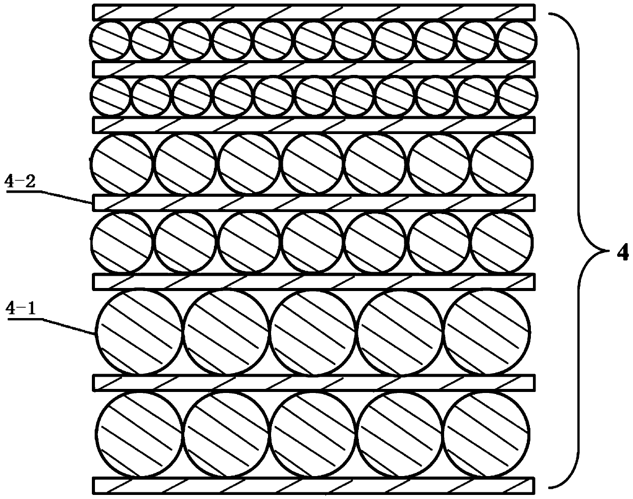
[0033] Such as figure 1 As shown, the p-type stacked graded bandgap silicon quantum dot multilayer film includes 6 layers of silicon quantum dot films 4-1 and 7 layers of silicon carbide films 4-2, and the thickness of the silicon carbide films 4-2 is 2 nm. Every two layers of silicon quantum dot films 4-1 have the same thickness, and there are three thickness specifications, which are 8 nm, 4 nm and 2 nm in turn, and the silicon quantum dot films 4-1 of the same thickne...


PUM

PropertyMeasurementUnit
Thicknessaaaaaaaaaa
Thicknessaaaaaaaaaa
Thicknessaaaaaaaaaa

Abstract

The invention discloses a p-type laminated graded band gap silicon quantum dot multilayer film, a preparation method and application thereof, and belongs to the field of photoelectric technology. Thep-type laminated graded band gap silicon quantum dot multilayer film includes six silicon quantum dot films, wherein every two silicon quantum dot films have the same thickness, the silicon quantum dot films of the same thickness specification are adjacent to each other, and adjacent silicon carbide films have one silicon quantum dot film therebetween. The preparation method comprises: growing a p-type laminated graded band gap silicon quantum dot multilayer film on an n-type silicon substrate 2 and an n-type silicon nanowire 3 by a plasma enhanced vapor deposition process. In this application, the p-type laminated graded band gap silicon quantum dot multilayer film is used to prepare a solar cell, which includes an Al electrode layer, an n-type silicon substrate, an n-type silicon nanowire, and a p-type laminated graded band gap silicon quantum dot multilayer film, a graphene layer and an Au electrode layer which are successively stacked. The graded band gap of the laminated silicon quantum dot multilayer film is configured to expand a light response range in an absorption layer so as to improve the photoelectric performance of a device.

Description

technical field [0001] The invention relates to a p-type laminated silicon quantum dot multilayer film with a gradual band gap and a preparation method and application thereof, belonging to the field of optoelectronic technology. Background technique [0002] With the continuous development of a new generation of solar cells, the nano-silicon structure is considered to be a material that can better adjust the band gap to achieve a wide spectral response. Among them, the heterojunction composed of a nano-silicon structure and a single crystal silicon substrate Solar cells have always been a research hotspot of widespread concern. However, on the one hand, due to the relatively small thickness of the active layer, the light absorption efficiency is relatively low. As a result, the photoelectric conversion efficiency of nano-silicon-monocrystalline silicon heterojunction solar cells is relatively low (5-6%). On the other hand, increasing the thickness of the active layer will...

Claims


Application Information

Patent Timeline
IPC IPC(8): H01L31/0224H01L31/028H01L31/0352H01L31/0745H01L31/18
CPCH01L31/035218H01L31/028H01L31/022425H01L31/0745H01L31/1804Y02E10/547Y02P70/50
Inventor 单丹周寿斌唐明军杨瑞洪曹蕴清钱松仇实陈雪圣
Owner JIANGSU HUAFU STORAGE NEW TECH DEV
Why Eureka
Try Eureka