A method for preparing large-area crack-free thick-film photonic crystals on porous substrates

A technology of photonic crystals and porous substrates, which is applied in the field of preparing large-area crack-free thick-film photonic crystals, and can solve problems such as cracks

Active Publication Date: 2021-08-27
SHANGHAI JIAO TONG UNIV
View PDF6 Cites 0 Cited by
  • Summary
  • Abstract
  • Description
  • Claims
  • Application Information

AI Technical Summary

Problems solved by technology

[0008] The purpose of the present invention is to provide a method for preparing a large-area crack-free thick-film photonic crystal on a porous substrate in order to overcome the above-mentioned defects in the prior art, which solves the problem of cracks in the preparation of large-area photonic crystals in the prior art. technical issues

Method used


Image

  • A method for preparing large-area crack-free thick-film photonic crystals on porous substrates
  • A method for preparing large-area crack-free thick-film photonic crystals on porous substrates
  • A method for preparing large-area crack-free thick-film photonic crystals on porous substrates

Examples


Embodiment 1

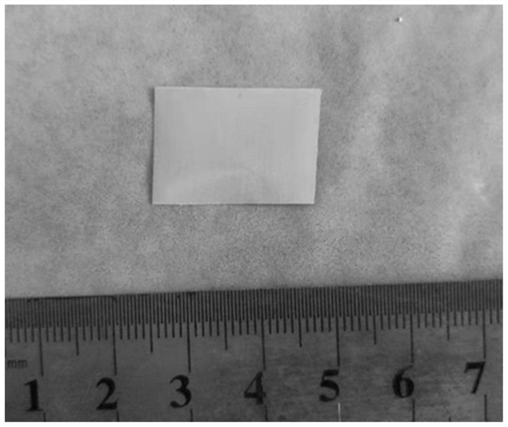
[0040] The method for preparing a silicon dioxide photonic crystal thick film with a thickness of 50 μm using a 500-mesh stainless steel mesh as a substrate is as follows:

[0041] 1) Take 1.0 g of silicon dioxide monodisperse microspheres with a particle size of 300 nm in a beaker, add 50 ml of absolute ethanol, and ultrasonically disperse for 30 min to form a uniform suspension with a mass concentration of 0.2%;

[0042] 2) take an area of ​​4cm 2 The 500-mesh stainless steel wire mesh was cleaned in absolute ethanol and acetone and placed in a drying oven to dry;

[0043] 3) Put the stainless steel wire mesh in the suspension, put it in an oven at 50°C, wait for 5 hours until the solvent of the suspension is completely volatilized, and then take it out to prepare a thick film of silicon dioxide photonic crystal with a thickness of 50 μm , and there is no crack on the surface, such as figure 1 shown.

Embodiment 2

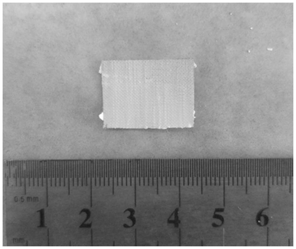
[0045] The method for preparing a 250 μm silicon dioxide photonic crystal thick film with a 150-mesh titanium mesh as a substrate is as follows:

[0046] 1) Take 2.0 g of silicon dioxide monodisperse microspheres with a particle size of 300 nm in a beaker, add 50 ml of absolute ethanol, and ultrasonically disperse for 30 minutes to form a uniform suspension with a mass concentration of 1%;

[0047] 2) take an area of ​​4cm 2 The 500-mesh stainless steel wire mesh was cleaned in absolute ethanol and acetone and placed in a drying oven to dry;

[0048] 3) Put the titanium mesh in the suspension and put it in an oven at 50°C. After 5 hours, until the solvent of the suspension is completely volatilized, then take it out to prepare a 250 μm thick film of silicon dioxide photonic crystal, and the surface no cracks as figure 2 shown.

Embodiment 3

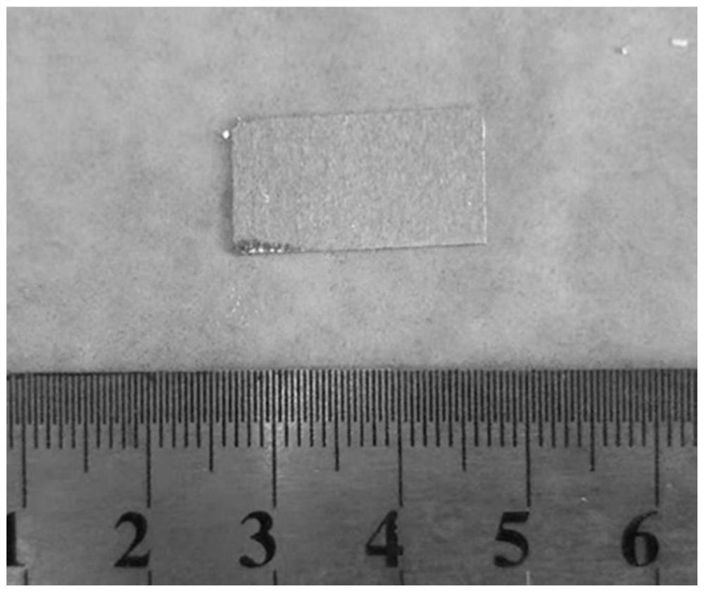
[0050] The method for preparing a polystyrene photonic crystal thick film with a thickness of 170 μm using carbon fiber paper as a substrate is as follows:

[0051] 1) Take 0.5g of polystyrene monodisperse microspheres with a particle size of 500nm in a beaker, add 200ml of deionized water, and ultrasonically disperse for 30min to form a uniform suspension with a mass concentration of 5%;

[0052] 2) take an area of ​​4cm 2 Carbon fiber paper with a thickness of 170 μm was washed in absolute ethanol and acetone respectively, and then dried in a drying oven;

[0053] 3) Put the carbon fiber paper in the suspension and put it in an oven at 55°C. After 24 hours, until the solvent of the suspension is completely volatilized, then take it out to prepare a 170 μm polystyrene photonic crystal thick film, and the surface no cracks as image 3 shown.

[0054] The reflection peak of the photonic crystal thick film is tested by a UV-visible spectrophotometer, and the result shows that...


PUM

PropertyMeasurementUnit
particle diameteraaaaaaaaaa
thicknessaaaaaaaaaa
thicknessaaaaaaaaaa

Abstract

The invention relates to a method for preparing a large-area crack-free thick-film photonic crystal on a porous substrate. A variety of porous substrates are used, placed in a suspension made of monodisperse microspheres, and self-assembled by vertical sedimentation In the method, as the solvent volatilizes, the monodisperse microspheres are arranged in the holes of the substrate to form a photonic crystal structure. Compared with the prior art, the present invention realizes the preparation of photonic crystals with a thickness ranging from 20 μm to 650 μm by changing the thickness of the substrate and the concentration of the suspension, and also realizes the preparation of photonic crystals with an area ranging from 0.1 cm to 650 μm by adjusting the area of ​​the substrate. 2 -100cm 2 The photonic crystal is prepared, and the surface of the photonic crystal has no obvious cracks.

Description

technical field [0001] The invention relates to the field of photonic crystal preparation, in particular to a method for preparing a large-area crack-free thick-film photonic crystal on a porous substrate. Background technique [0002] Materials with a photonic band-gap (Photonic Band-Gap) are also called photonic crystals, which refer to a class of materials whose dielectric constant (refractive index) changes periodically on the submicron scale. The concept of photonic crystals was first proposed independently by Yablonovitch and John in 1987. It was derived from the analogy of the traditional crystal concept: in a crystal, the size is 10 - 10 The periodic arrangement of atoms in m can diffract X-rays; in photonic crystals, the size is 10 -7 The periodic structure of m can diffract visible light. In 1999, American Science magazine listed photonic crystals as one of the six research hotspots in the future, which heralded the broad prospect of photonic crystal research. ...

Claims


Application Information

Patent Timeline
Patent Type & Authority Patents(China)
IPC IPC(8): C30B7/04C30B7/06C30B29/64C30B29/18C30B29/54
CPCC30B7/04C30B7/06C30B29/18C30B29/54C30B29/64
Inventor 胡晓斌蔡子贺林升炫肖佳佳
Owner SHANGHAI JIAO TONG UNIV
Why Eureka
Try Eureka