Fast recovery diode and manufacturing method thereof

A technology of rapid recovery and manufacturing method, applied in the field of diodes, can solve the problems of high switching loss and large forward voltage of diodes, and achieve the effects of reducing switching loss, reducing forward voltage and improving practicality.

Inactive Publication Date: 2020-04-10
ZHANGJIAGANG EVER POWER SEMICON
View PDF0 Cites 0 Cited by
  • Summary
  • Abstract
  • Description
  • Claims
  • Application Information

AI Technical Summary

Problems solved by technology

[0004] The purpose of the present invention is to provide a fast recovery diode and its manufacturing method to solve the problems of large forward voltage and high switching loss of conventional diodes

Method used


Image

  • Fast recovery diode and manufacturing method thereof
  • Fast recovery diode and manufacturing method thereof

Examples


Embodiment 1

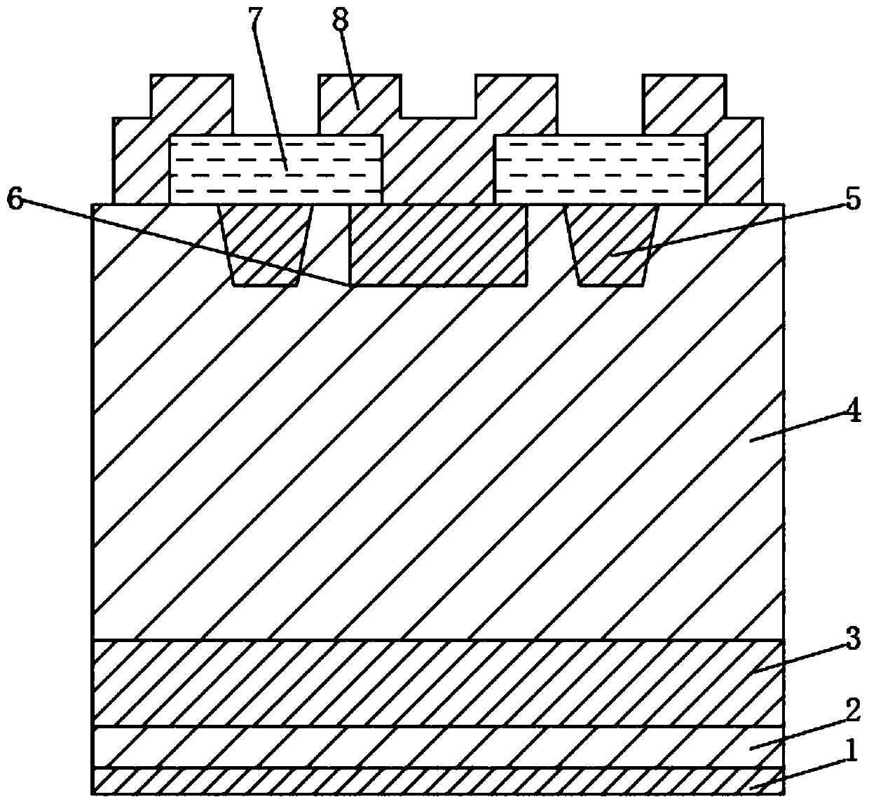
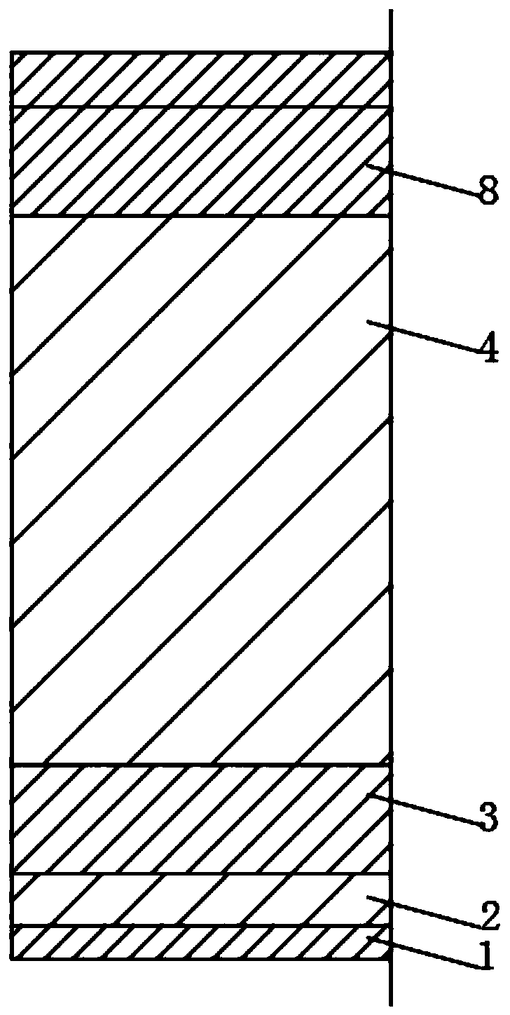
[0024] see figure 1 and figure 2 , the present invention provides a technical solution: a fast recovery diode, comprising a collector 1, an N-type buffer 2 is arranged on the collector 1, an N-type substrate 3 is arranged on the N buffer 2, and an N-type substrate 3 The N-field stop layer 4 is arranged on the N-field stop layer 4, and the P base region 5 and the P+ ohmic contact region 6 are arranged on the N-field stop layer 4. On the N-field stop layer 4, on the P base region 5 and on the P+ ohmic contact region 6 Both are provided with borophosphosilicate glass 7 and metal layer 8, and the metal layer 8 and borophosphoric acid glass 7 are arranged in close contact.

[0025] Fast recovery diodes are fabricated as follows: chip preparation, boron diffusion, oxidation, growth of Si 3 N 4 , photolithography, engraved passivation Si 3 N 4 or SiO 2 , Mesa corrosion, oxidation, etch and etch passivation of silicon groove 3 N 4 or SiO 2 , oxidize, corrode SiO 2 , oxidati...

Embodiment 2

[0038] see figure 1 and figure 2 , the present invention provides a technical solution: a fast recovery diode, comprising a collector 1, an N-type buffer 2 is arranged on the collector 1, an N-type substrate 3 is arranged on the N buffer 2, and an N-type substrate 3 The N-field stop layer 4 is arranged on the N-field stop layer 4, and the P base region 5 and the P+ ohmic contact region 6 are arranged on the N-field stop layer 4. On the N-field stop layer 4, on the P base region 5 and on the P+ ohmic contact region 6 Both are provided with borophosphosilicate glass 7 and metal layer 8, and the metal layer 8 and borophosphoric acid glass 7 are arranged in close contact.

[0039] Fast recovery diodes are fabricated as follows: chip preparation, boron diffusion, oxidation, growth of Si 3 N 4 , photolithography, engraved passivation Si 3 N 4 or SiO 2 , Mesa corrosion, oxidation, etch and etch passivation of silicon groove 3 N 4 or SiO 2 , oxidize, corrode SiO 2 , oxidati...


PUM


Abstract

The invention discloses a fast recovery diode. The fast recovery diode comprises a collector, an N-type buffer region is arranged on the collector, and an N-type substrate is arranged on the N bufferregion. An N-field cut-off layer is arranged on the N-type substrate, a P base region and a P + ohmic contact region are arranged on the N-field cut-off layer, boron phosphorosilicate glass and a metal layer are arranged on the N-field cut-off layer, the P base region and the P + ohmic contact region, and the metal layer is tightly attached to the boron phosphorosilicate glass. According to the present invention, the switching loss is reduced, and the N-type buffer layer is optimized; and by adopting the thinner N-type substrate, the active surface area is increased, the current density is improved by 30%, the service life of longitudinal carriers is prolonged, a forward voltage is reduced, and the practicability of a whole component is improved.

Description

technical field [0001] The invention relates to the technical field of diodes, in particular to a fast recovery diode and a manufacturing method thereof. Background technique [0002] With the development of power electronics technology, the research and development of power semiconductor devices has become an important independent device, which is also developing in the direction of large capacity, high frequency, high efficiency and low cost. [0003] Due to the large amount of forward and switching consumption of traditional diode components, the performance of various aspects is greatly reduced when used, and the current density is small, and the lifetime of longitudinal carriers is low, causing unnecessary troubles in actual work. Contents of the invention [0004] The purpose of the present invention is to provide a fast recovery diode and its manufacturing method to solve the problems of large forward voltage and high switching loss of conventional diodes. [0005]...

Claims


Application Information

Patent Timeline
Patent Type & Authority Applications(China)
IPC IPC(8): H01L21/329H01L29/868H01L29/06
CPCH01L29/0684H01L29/6609H01L29/868
Inventor 周炳赵承杰许新佳
Owner ZHANGJIAGANG EVER POWER SEMICON
Why Eureka
Try Eureka