Insulating layer buried transistor structure and device

An insulating layer and transistor technology, applied in the direction of transistors, semiconductor devices, electrical components, etc., can solve the problems of substrate size limitation, large leakage current, low efficiency, etc., to improve the operating frequency range, improve operating power, and work efficiency Enhanced effect

Active Publication Date: 2020-04-28
成都挚信电子技术有限责任公司
View PDF11 Cites 4 Cited by
  • Summary
  • Abstract
  • Description
  • Claims
  • Application Information

AI Technical Summary

Problems solved by technology

However, the existing GaAspHEMT transistors have the following disadvantages: large leakage current, including the leakage current between the gate and the source, and the two-dimensional electron gas leaks to the GaAs substrate through the undoped GaAs / AlGaAs superlattice buffer layer current; the efficiency of GaAs pHEMT transistors is significantly reduced due to the existence of leakage current; the stackability of GaAs pHEMT devices is not good due to the existence of leakage current
GaN (GaN-on-SiC) on silicon carbide (SiC) substrates developed on this basis, and GaN (GaN-on-Si) on Si (silicon) substrates, the main advantage of SiC substrates is the heat dissipation characteristics , GaN (GaN-on-SiC) on silicon carbide (SiC) substrates is mainly suitable for high-frequency, high-voltage, high-temperature applications, and its main disadvantages are: the size of the substrate is limited, the cost is relatively high, and it is difficult to integrate with CMOS, etc. Si-based technology integration
However, GaN (GaN-on-Si) on Si (silicon) substrates also has some problems, which are manifested in: poor high-frequency characteristics, poor reliability, large leakage current and low efficiency

Method used


Image

  • Insulating layer buried transistor structure and device
  • Insulating layer buried transistor structure and device
  • Insulating layer buried transistor structure and device

Examples


Embodiment 1

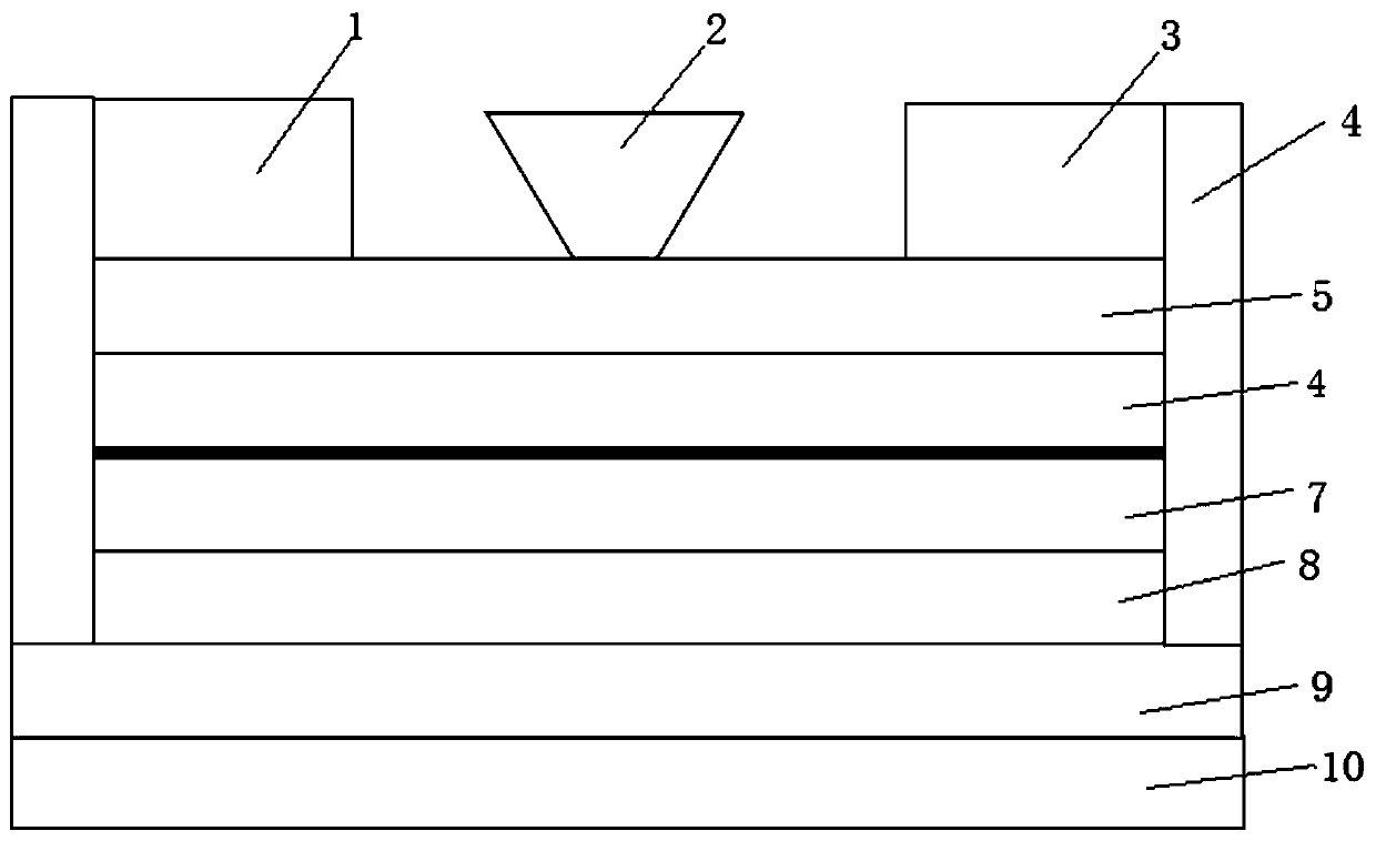
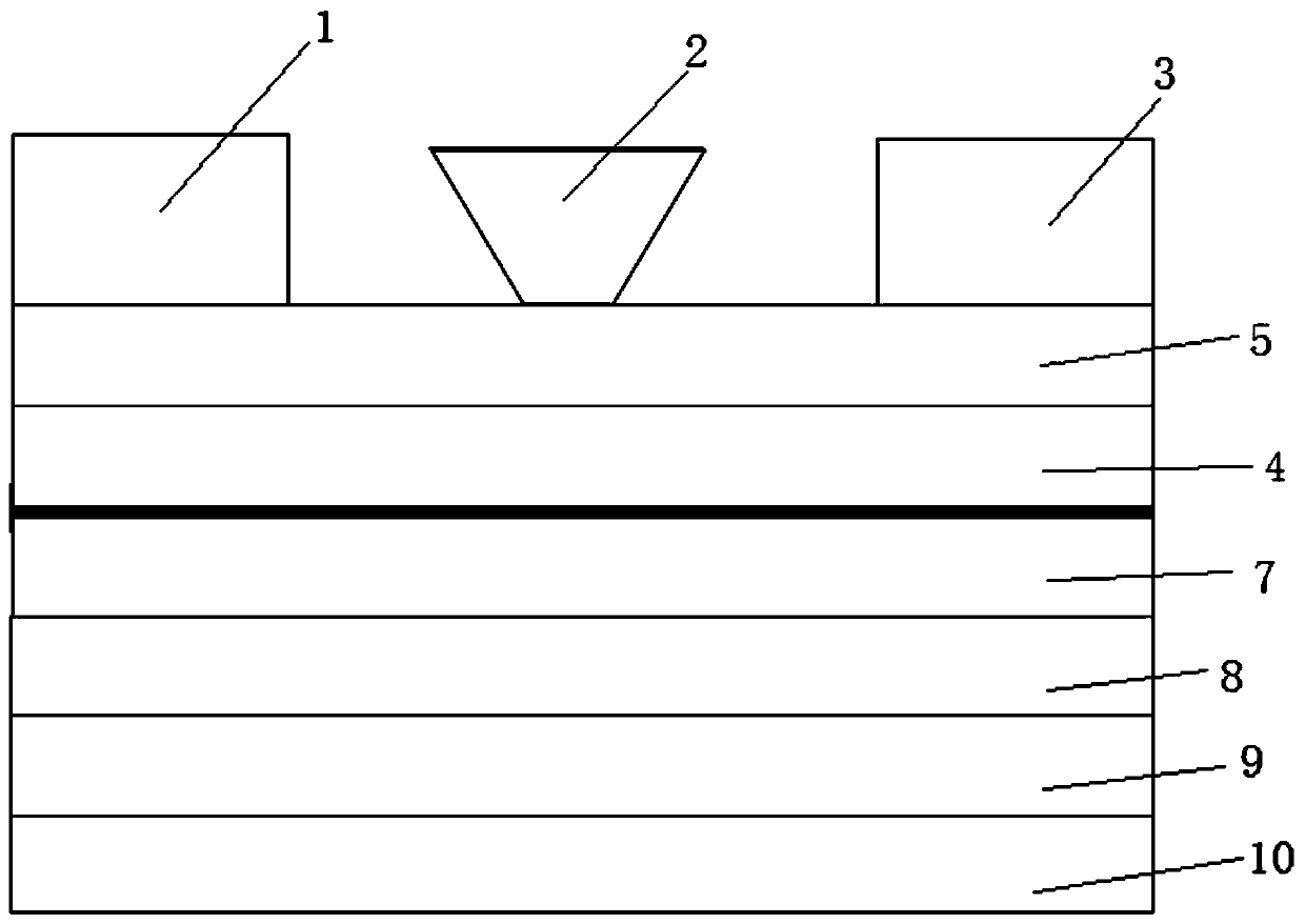
[0040]This embodiment discloses a transistor structure buried in an insulating layer 9, including a semiconductor substrate, a source 1, a gate 2, and a drain 3, and the semiconductor substrate includes a supporting substrate 10, a channel layer 7, and an isolation layer 4 and a barrier layer 5, the channel layer 7, the isolation layer 4 and the barrier layer 5 are all III-V group compound semiconductor film layers, and the channel layer 7, The isolation layer 4 and the barrier layer 5; the source 1 and the drain 3 are arranged on both sides of the barrier layer 5 and are in contact with the barrier layer 5; the gate 2 is arranged on the source 1 Between the drain electrode 3 and the barrier layer 5; an insulating layer 9 is provided between the supporting substrate 10 and the channel layer 7; the insulating layer 9 is an oxide layer; on the supporting substrate 10 An insulating layer 9 is arranged between the channel layer 7, which is mainly used to block substrate leakage, i...

Embodiment 2

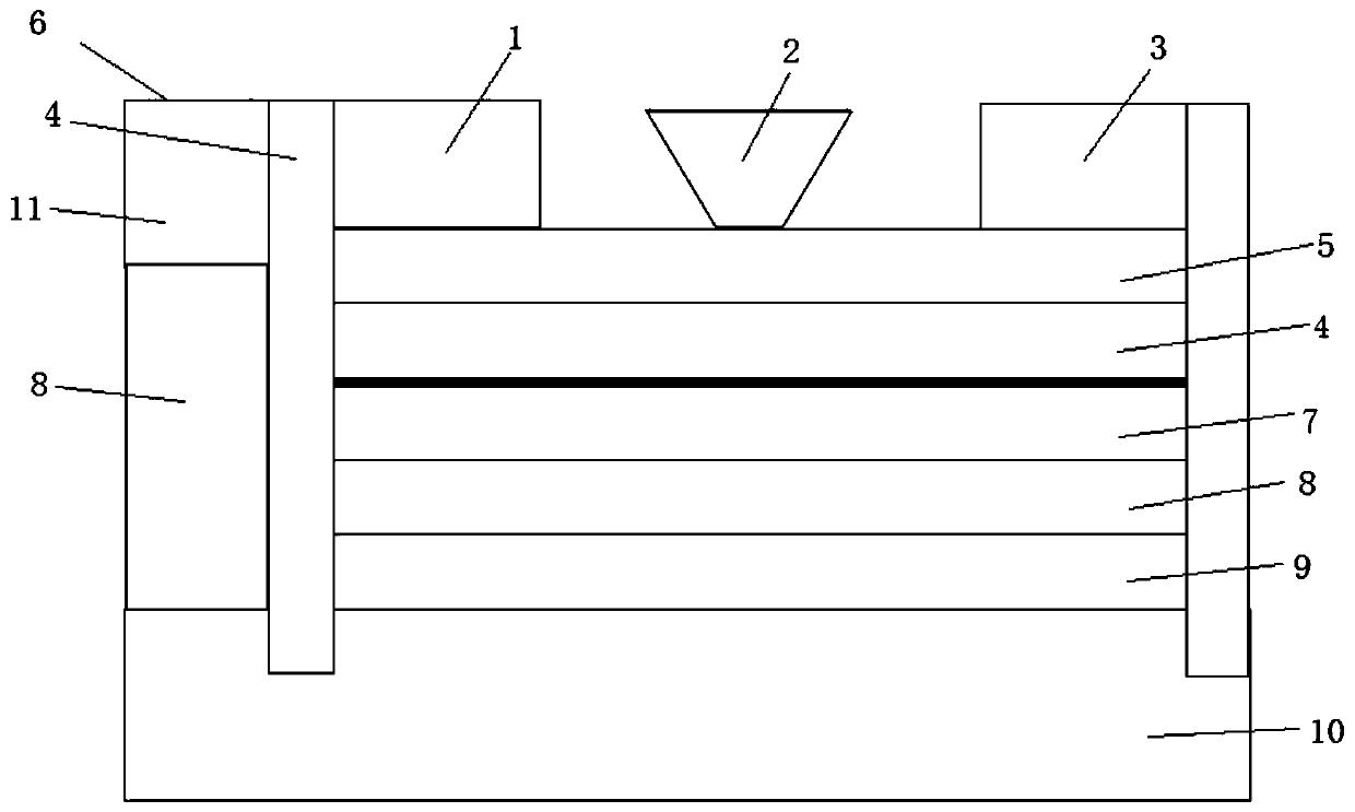
[0042] This embodiment is based on the first embodiment, and discloses a transistor structure buried with insulating layers 9, the insulating layers 9 and the buffer layers 8 are arranged alternately; the insulating layers 9 are provided with at least one layer; the The buffer layer 8 is provided with at least one layer; the back gate control electrode 12 includes a contact layer 11 and a buffer layer 8; the contact layer 11 is grown on the buffer layer 8, and the back gate control electrode 12 is provided with a buffer layer 8, A layer of buffer layer 8 is arranged on the insulating layer 9, and two layers of buffer layer 8 are arranged, mainly for the transition and buffering of growing high-quality crystals, avoiding the occurrence of crystal cracks and deformation caused by direct growth of crystals, and the material of buffer layer 8 The lattice constant is between the lattice constants of the semiconductor material of the channel layer 7 and the semiconductor material of ...

Embodiment 3

[0044] This embodiment is based on Embodiment 1 and Embodiment 2, and discloses a scene switching in transistors realized by controlling the threshold of the back gate gate, using the level of the threshold voltage of the back gate gate 12 transistors to substantially adapt to different The application environment, and the level of the threshold voltage required by different scenarios is controlled through the back gate, and different scenarios are switched. It can be widely used in different scenarios such as the 5th generation mobile communication and the Internet of Everything IoT.


PUM


Abstract

The invention discloses an insulating layer buried transistor structure and a device. The insulating layer buried transistor structure comprises a semiconductor substrate, a source electrode, a grid electrode, and a drain electrode, wherein a channel layer, an isolation layer, and a barrier layer are sequentially grown on a supporting substrate; the grid electrode is arranged between the source electrode and the drain electrode; an insulating layer is arranged between the supporting substrate and the channel layer; and the supporting substrate is a substrate compatible with an insulating layergrowth process. The transistor comprises a back gate control electrode and an isolation layer, wherein the back gate control electrode is isolated from the channel layer through an isolation layer. The beneficial effects are that the leakage of the substrate is effectively blocked, the leakage current among the grid electrode, the source electrode and the supporting substrate is improved / controlled, and the noise coefficient is reduced; crystal chapping deformation and reliability reduction caused by growth of lattice mismatch materials are avoided; and the threshold voltage can be controlledthrough the back gate control electrode, and the leakage current is further reduced, so that various novel functional devices are developed.

Description

technical field [0001] The invention relates to the field of transistors, in particular to an insulating layer buried type transistor structure and device. Background technique [0002] The existing III-V compound semiconductors include GaAs, GaN, InP and other types. In the GaAs pHEMT substrate structure, the undoped InGaAs layer and the AlGaAs layer form a heterojunction at the interface to generate a two-dimensional electron gas. The gate controls the barrier height, and when the gate reaches a certain bias voltage, the two-dimensional electron gas tunnels across the barrier to form a current between the source and drain. In order to prevent the current from leaking into the GaAs substrate, an undoped GaAs / AlGaAs superlattice buffer layer is added. However, the existing GaAspHEMT transistors have the following disadvantages: large leakage current, including the leakage current between the gate and the source, and the two-dimensional electron gas leaks to the GaAs substr...

Claims


Application Information

Patent Timeline
Patent Type & Authority Applications(China)
IPC IPC(8): H01L29/778H01L29/423H01L29/10H01L29/06
CPCH01L29/7783H01L29/1029H01L29/0638H01L29/42316
Inventor 黄永锋殷玉喆何力温礼瑞曾志学孙德许苏凌
Owner 成都挚信电子技术有限责任公司
Why Eureka
Try Eureka