Self-aligned gate gallium nitride enhanced vertical power device based on suspension field plate
A vertical power device, self-aligned technology, used in semiconductor devices, semiconductor/solid-state device manufacturing, electrical components, etc. Effects of cost reduction, high process compatibility, and low on-resistance
- Summary
- Abstract
- Description
- Claims
- Application Information
AI Technical Summary
Problems solved by technology
Method used
Image

Examples
Embodiment 1
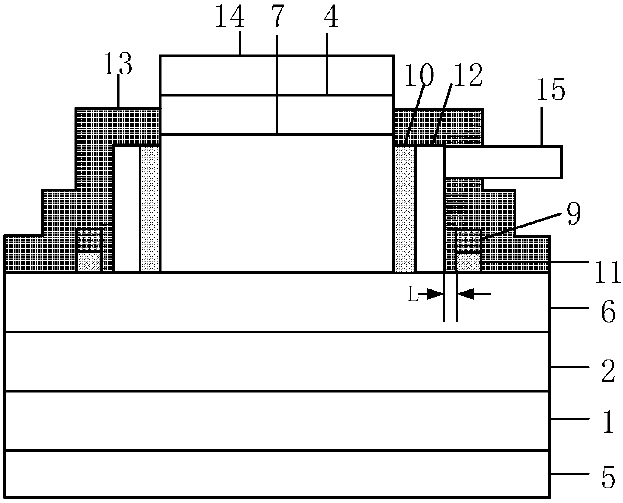
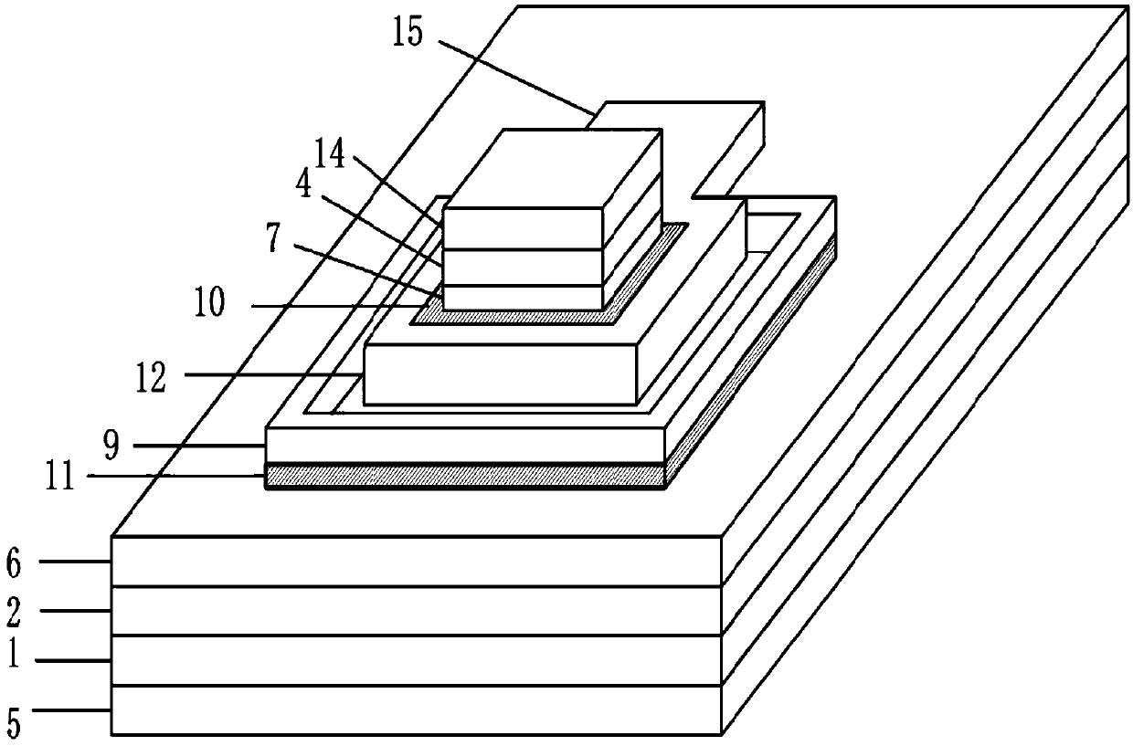
[0038] See figure 1 and figure 2 , figure 1 A schematic structural diagram of a self-aligned gate GaN-enhanced vertical power device based on a floating field plate provided by an embodiment of the present invention, figure 2 A schematic diagram of a three-dimensional structure of a self-aligned gate GaN-enhanced vertical power device based on a floating field plate provided by an embodiment of the present invention (the third dielectric layer is not included). The self-aligned gate GaN-enhanced vertical power device based on a floating field plate comprises: a self-supporting Si-doped GaN substrate 1; a drain 5 located below the self-supporting Si-doped GaN substrate 1; an n-type GaN Layer 2, located on the self-supporting Si-doped GaN substrate 1; n-type GaN transition layer 6, located on the n-type GaN layer 2; n-type GaN channel layer 7, located on the n-type GaN transition layer 6; A dielectric layer 10 is located on the n-type GaN transition layer 6; a gate 12 is lo...
Embodiment 2
[0057] See Figure 3a-Figure 3l , Figure 3a-Figure 3l A schematic flow chart of a method for manufacturing a self-aligned gate GaN-enhanced vertical power device based on a floating field plate provided by an embodiment of the present invention, including steps:
[0058] S1. Using molecular beam epitaxy (Molecular Beam Epitaxy, referred to as MBE) process, grow n-type GaN material on a self-supporting Si-doped GaN substrate 1, see Figure 3a ;include:
[0059] S11. Growing a heavily doped n-type GaN layer 2 on a self-supporting Si-doped GaN substrate 1, wherein the thickness of the n-type GaN layer 2 is 100-300 nm, the doping element is Si, and the doping concentration is 1× 10 18 cm -3 ~1×10 19 cm -3 ;
[0060] S12. Growing a low-doped n-type GaN layer 3 on the n-type GaN layer 2, wherein the thickness of the n-type GaN layer 3 is 6-8 μm, the doping element is Si, and the doping concentration is 1×10 15 cm -3 ~1×10 17 cm -3 ;
[0061] S13. Growing an n-type GaN c...
PUM
| Property | Measurement | Unit |
|---|---|---|
| Thickness | aaaaa | aaaaa |
| Thickness | aaaaa | aaaaa |
| Thickness | aaaaa | aaaaa |
Abstract
Description
Claims
Application Information
 - Generate Ideas
- Intellectual Property
- Life Sciences
- Materials
- Tech Scout
- Unparalleled Data Quality
- Higher Quality Content
- 60% Fewer Hallucinations
Browse by: Latest US Patents, China's latest patents, Technical Efficacy Thesaurus, Application Domain, Technology Topic, Popular Technical Reports.
© 2025 PatSnap. All rights reserved.Legal|Privacy policy|Modern Slavery Act Transparency Statement|Sitemap|About US| Contact US: help@patsnap.com