MoS2 phototransistor capable of improving photoelectric detection performance and manufacturingmethod thereof

A phototransistor and photodetection technology, applied in the field of photodetection, can solve the problems of high cost and cumbersome preparation methods, achieve the effects of alleviating photoresponsivity and photoresponse speed, improving photoresponsivity, and breaking through technical barriers

Inactive Publication Date: 2020-05-29
CHANGCHUN UNIV OF SCI & TECH
View PDF5 Cites 5 Cited by
  • Summary
  • Abstract
  • Description
  • Claims
  • Application Information

AI Technical Summary

Problems solved by technology

This method constructs a traditional three-terminal phototransistor with asymmetric electrodes, which inevitably leads to cumbersome preparation methods and high costs.

Method used


Image

  • MoS2 phototransistor capable of improving photoelectric detection performance and manufacturingmethod thereof
  • MoS2 phototransistor capable of improving photoelectric detection performance and manufacturingmethod thereof
  • MoS2 phototransistor capable of improving photoelectric detection performance and manufacturingmethod thereof

Examples


Embodiment Construction

[0038] The present invention will be described in further detail below in conjunction with the accompanying drawings and embodiments.

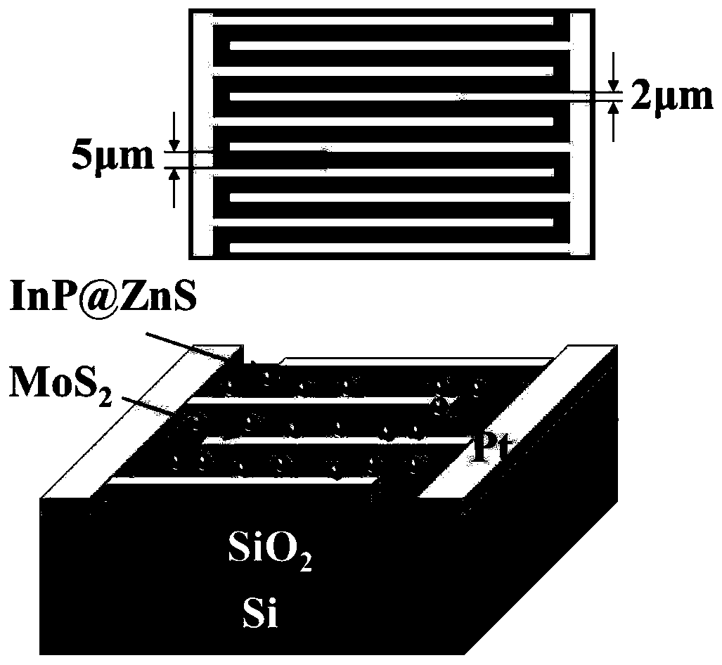
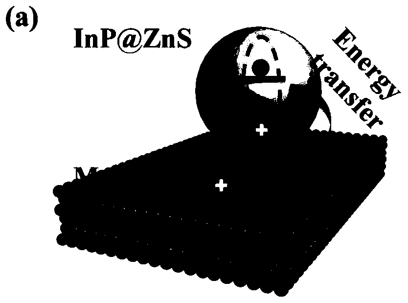
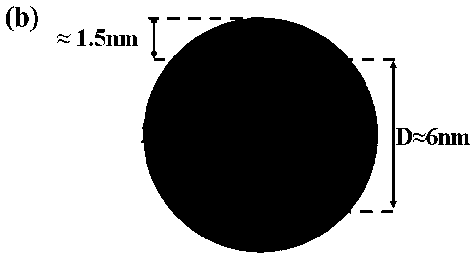
[0039] like figure 1 As shown, a MoS with improved photodetection performance 2 A phototransistor comprising: Si / SiO 2 Substrate, bilayer MoS 2 Thin films, Pt electrodes, InP@ZnS quantum dots and silver films; multiple sheets of the bilayer MoS 2 The film is randomly arranged on the Si / SiO 2 The upper surface of the substrate; wherein the bilayer MoS 2 The film has a triangular structure. The Pt electrode is fabricated on the bilayer MoS 2 Thin films and Si / SiO 2 The upper surface of the substrate is used as the drain source electrode; the Pt electrode is an interdigitated electrode with a thickness of 50nm and a width of 2 μm to realize the surface plasmon effect; the finger length of the Pt electrode is 300 μm, and the wide distance between the two electrodes is 5 μm ; this bridge-like MoS 2 They are connected together under differe...


PUM

PropertyMeasurementUnit
thicknessaaaaaaaaaa
widthaaaaaaaaaa
sizeaaaaaaaaaa

Abstract

The invention discloses a MoS2 phototransistor capable of improving photoelectric detection performance and a manufacturing method thereof, and relates to the technical field of photoelectric detection. Based on a novel 2D/0D hybrid interdigital phototransistor, high responsivity, a ultrafast response speed and self-powered photoelectric detection performance are realized. The phototransistor comprises a Si/SiO2 substrate, double-layer MoS2 thin films, a Pt electrode, InP@ZnS quantum dots and a silver film, and the plurality of double-layer MoS2 thin films are arranged on an upper surface of the Si/SiO2 substrate; a Pt electrode is manufactured on the upper surfaces of the double-layer MoS2 thin films and the Si/SiO2 substrate to serve as a drain-source electrode; the Pt electrode is an interdigital electrode, a thickness of the Pt electrode is 50nm, a width of the Pt electrode is 2 microns, a finger length of the Pt electrode is 300 microns, and a width distance between the two electrodes is 5 microns; the InP@ZnS quantum dots are manufactured on the surfaces of the Si/SiO2 substrate, the double-layer MoS2 thin films and the Pt electrode; and the silver film is manufactured on a back surface of the Si/SiO2 substrate to serve as a back gate electrode. Due to a design of a 2-micron interdigital Pt electrode, a plasma resonance effect can be achieved, and photoresponsivity is improved; and introduction of an asymmetric Pt/MoS2 Schottky barrier can effectively balance a dilemma of the photoresponsivity and a photoresponse speed.

Description

technical field [0001] The invention relates to the technical field of photoelectric detection, in particular to a MoS that improves the performance of photoelectric detection 2 Phototransistors and methods of making them. Background technique [0002] In recent years, phototransistors based on two-dimensional (2D) materials have become the research frontier in the field of photodetection, with applications in optical computing, optical logic, optical communication, and emerging artificial neuromorphic simulations. In order to ensure the detection of weak signals and the undistorted output of high-frequency signals, an ideal photodetector device should have both high responsivity and fast response speed detection performance. Molybdenum disulfide (MoS 2 ) as a member of typical transition metal dichalcogenides (TMDCs), due to the potential advantages of high in-plane carrier mobility, tunable bandgap, inherent flexibility, and good compatibility with other semiconductor ma...

Claims


Application Information

Patent Timeline
Patent Type & Authority Applications(China)
IPC IPC(8): H01L31/0352H01L31/0224H01L31/032H01L31/113H01L31/18B82Y30/00B82Y40/00
CPCB82Y30/00B82Y40/00H01L31/022408H01L31/032H01L31/035218H01L31/03529H01L31/1136H01L31/18Y02P70/50
Inventor 石凯熙李金华翟英娇楚学影柳琦
Owner CHANGCHUN UNIV OF SCI & TECH
Why Eureka
Try Eureka