
High-voltage PMOS drive circuit

A drive circuit, high-voltage technology, applied in the direction of logic circuit, logic circuit interface device, eliminating voltage/current interference, etc., can solve the problems of pulse width not too small, easy to be interfered, and loss, etc. Conduction loss, low cost effect

Pending Publication Date: 2020-06-05
苏州源特半导体科技有限公司
View PDF0 Cites 3 Cited by
  • Summary
  • Abstract
  • Description
  • Claims
  • Application Information

AI Technical Summary

Problems solved by technology

If there is no voltage stabilization effect of an external capacitor, the voltage at VCAP can drop to 0V, and the working voltage of the load element of the latch, buffer and pulse potential shifting circuit reaches 100V, which is directly broken down and damaged
[0008] 2. Voltage limitation at nodes A and B is achieved by diode conduction, there is D1 clamp With NM1, D2 clamp The phenomenon of simultaneous conduction with NM2 has loss, so NM1 and NM2 are controlled by narrow pulse voltage to save power consumption. The smaller the pulse width, the smaller the loss; however, it takes time for the voltage at nodes A and B to establish, pulse The width should not be too small
[0009] 3. After the driving pulses of NM1 and NM2 disappear, the voltage at node B is maintained by the latch itself, which is easy to be disturbed. The positive feedback resistance value can be reduced to improve the anti-interference ability, but there will be more loss

Method used


Image

  • High-voltage PMOS drive circuit
  • High-voltage PMOS drive circuit
  • High-voltage PMOS drive circuit

Examples


Embodiment 1

[0044] Such as Figure 6 Shown is a circuit block diagram of the high-voltage PMOS drive circuit of the present invention, including: a pulsed potential shift circuit 101 , a latch 102 , a buffer 103 and a clamper 104 . The pulsed potential shift circuit 101 receives the low-end logic signal Lin to generate a high-end voltage difference signal; the latch 102 converts the high-end voltage difference signal into a high-end logic level, and locks the level voltage through positive feedback; the buffer 103 receives the lock The high-end logic level provided by the register generates a high-end drive voltage with sufficient drive capability for driving high-voltage PMOS transistors. The required drive capability is determined by the size and switching speed of the PMOS transistor. The high-low voltage difference of the high-end drive voltage is determined by the PMOS The working condition of the tube is determined; the clamper 104 provides the negative terminal voltage for the latc...

Embodiment 2

[0064] On the basis of Embodiment 1, the traditional pulse-type potential shifting circuit is improved, the shifting pulse generation circuit can be dispensed with, and the pulse width of the low-end logic signal Lin can be directly used for driving, and it is no longer necessary to generate double pulse widths for shifting control , and there is no common phenomenon of the traditional solution, even the latch in the first embodiment can be removed, and a high signal-to-noise ratio can be ensured.

[0065] Such as Figure 8 Shown is the circuit block diagram of this embodiment. The present invention is more preferably a high-voltage PMOS drive circuit with a double-layer potential shift circuit, including: a double-layer potential shift circuit 201 , a buffer 103 , and a clamper 104 . The double-layer potential shifting circuit 201 receives the low-end logic signal Lin and the bias voltage provided by the clamper 104, and outputs a high-side logic level. The bias voltage contr...

Embodiment 3

[0072] The basic structures of the NOT gates that make up the buffer 103 in Embodiment 1 and Embodiment 2 are as follows: Figure 11 As shown, the source of NMa is connected to the negative power supply terminal of the buffer, which is at a high voltage, which requires a high-voltage isolation NMOS transistor to realize, but there is no such device in many semiconductor processes. Therefore, in this embodiment, the buffer is implemented by a double-layer inverter, which is a buffer that does not require a high-voltage isolation NMOS transistor, thereby reducing the requirements for semiconductor technology.

[0073] Familiar with the clamping principle of the double-layer potential shifting circuit in the second embodiment, a double-layer inverter can be produced in a similar way, such as Figure 12 As shown in 303, the double-layer inverter of this embodiment includes a PMOS inverting load transistor PM3, an NMOS inverting control transistor NM3, and a PMOS inverting clamp tr...


PUM


Abstract

The invention discloses a high-voltage PMOS drive circuit. The circuit comprises a double-layer potential translation circuit, a clamper and a buffer. The double-layer potential translation circuit receives a low-end logic signal and a bias voltage provided by the clamper and outputs a high-end logic level to the buffer, and the buffer generates a high-end driving voltage as an output of the high-voltage PMOS drive circuit to control on and off of a high-voltage PMOS transistor. The output end of the clamper provides a negative end voltage for the buffer, so that the buffer works in a safe area, and the clamper provides a bias voltage for the double-layer potential translation circuit. Under the condition that an external capacitor is not needed, the voltages of a load element, a latch andthe buffer are all controlled within a safe working range, the integration level is high, and the cost is low. The voltage difference generated on the load element in the double-layer potential translation circuit is stable and reliable and is not easy to interfere with, and a latch required in the traditional technology can be omitted, so that the cost is saved.

Description

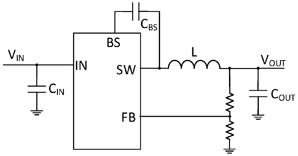
technical field [0001] The invention relates to a MOS transistor drive circuit in the field of integrated circuits, in particular to a high-voltage PMOS drive circuit. Background technique [0002] With the further development of the high-voltage BCD process in recent years, in addition to the long-popular high-voltage NMOS devices with low internal resistance, more and more high-voltage semiconductor processes have also designed high-voltage PMOS devices with low internal resistance. This key device can be used to design Some more competitive low-power switching power supply chips have simpler peripherals. For example, using conventional technology, only such as figure 1 For the high-voltage input step-down Buck switching power supply shown, since the NMOS driving voltage must be higher than the input voltage, this kind of Buck requires an external bootstrap capacitor C between the ports SW and BS. BS To supply power for the high-voltage bootstrap circuit, if the semicond...

Claims


Application Information

Patent Timeline
IPC IPC(8): H03K19/0175H03K19/003H03K19/00
CPCH03K19/001H03K19/0013H03K19/0016H03K19/00307H03K19/00315H03K19/00353H03K19/00361H03K19/017518
Inventor 唐盛斌
Owner 苏州源特半导体科技有限公司
Learn More