Amorphous alloy coloring method, amorphous alloy and application of amorphous alloy coloring method
An amorphous alloy and amorphous technology, applied in the coloring method of amorphous alloy, its amorphous alloy and its application field, can solve the problems of time-consuming nanostructure lithography, complicated oxidation process, and reduced material performance, etc., and achieve processing speed Fast, high-precision, high-resolution effects
- Summary
- Abstract
- Description
- Claims
- Application Information
AI Technical Summary
Problems solved by technology
Method used
Image
Examples
Embodiment 1
[0078] This example is used to illustrate the coloring method of the amorphous alloy of the present invention.
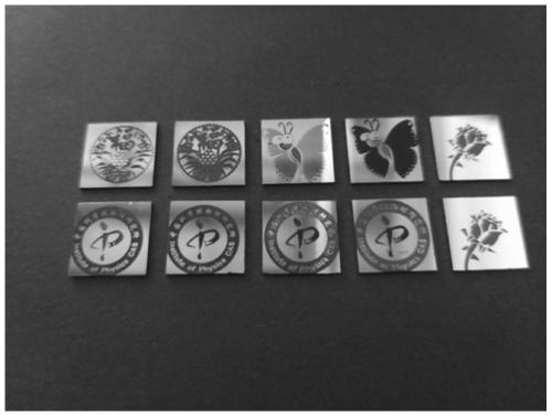
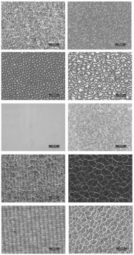
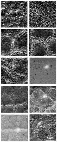
[0079] Ion beam sputtering on a silicon substrate is selected, and the vacuum degree is 2.4×10 -4 Under the Pa argon environment, the main cathode current is 6.5A, the screen grid voltage is 50V, the ion beam current is 80mA, the ion energy is 750eV, the working time is 2350s, and the same time is plated four times. Prepare Zr with a thickness of 1.5 microns according to the above parameters 46 Cu 46 al 8 (According to atomic percentage) amorphous alloy film. The surface of the film has a mirror surface that is smooth and flat at the atomic level. Place the thin film sample on the laser processing platform with the mirror facing up, using a nanosecond laser with an output power of 20W, a wavelength of 1064nm, a focus spot diameter of 0.05mm, and a pulse width range of 2-250ns. It performs scan and scribe surface processing or fill and scribe processing (the rou...
Embodiment 2
[0085] This example is used to illustrate the coloring method of the amorphous alloy of the present invention.
[0086] Ion beam sputtering on a silicon substrate is selected, and the vacuum degree is 2.4×10 -4 In the Pa argon environment, the main cathode current is 6.5A, the screen grid voltage is 50V, the ion beam current is 80mA, the ion energy is 750eV, the working time is 2350s, and the same time is plated 6 times to prepare Zr with a thickness of 2 microns. 46 Cu 46 al 8 (According to atomic percentage) amorphous alloy film. The surface of the film has a mirror surface that is smooth and flat at the atomic level. The thin film sample is placed on the laser processing platform with the mirror facing up, using a picosecond laser with an output power of 20W, a wavelength of 355nm, a focused spot diameter of 0.02mm, and a pulse width of 7ps. By fixing the defocus amount as 1 mm, selecting a power factor of 50 to 100%, a scanning speed of 10 to 8000 mm / s, a repetition fr...
Embodiment 3
[0090] This example is used to illustrate the coloring method of the amorphous alloy of the present invention.
[0091] Al with a thickness of 40 microns 86 Ni 7 Y 5 co 1 La 1 The amorphous alloy strip is ultrasonically cleaned with alcohol, and then the surface of the amorphous alloy strip is treated with a nanosecond laser. The processing and detection methods are as in Example 1. The relationship between the resulting color and the processing parameters is shown in Table 3.
[0092] The relationship between the color of the surface of the amorphous alloy strip and the treatment method in Table 3 Example 3
[0093]
PUM
| Property | Measurement | Unit |
|---|---|---|
| Thickness | aaaaa | aaaaa |
| Thickness | aaaaa | aaaaa |
Abstract
Description
Claims
Application Information
 - R&D
- Intellectual Property
- Life Sciences
- Materials
- Tech Scout
- Unparalleled Data Quality
- Higher Quality Content
- 60% Fewer Hallucinations
Browse by: Latest US Patents, China's latest patents, Technical Efficacy Thesaurus, Application Domain, Technology Topic, Popular Technical Reports.
© 2025 PatSnap. All rights reserved.Legal|Privacy policy|Modern Slavery Act Transparency Statement|Sitemap|About US| Contact US: help@patsnap.com


