

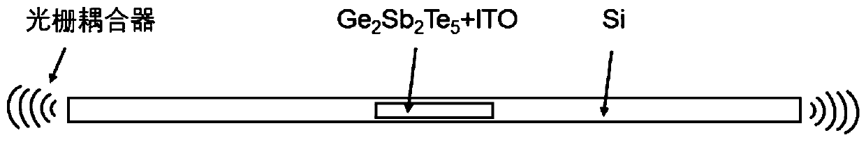
On-chip photon multi-stage switch based on Si-Ge2Sb2Te5 mixed waveguide
A si-ge2sb2te5, mixed wave technology, applied in the direction of optical waveguide light guide, optical waveguide coupling, light guide, etc., can solve the problems of large static power consumption, stability problems, small refractive index adjustment range, etc., to improve conversion efficiency, The effect of reducing energy consumption
- Summary
- Abstract
- Description
- Claims
- Application Information
AI Technical Summary
Problems solved by technology
Method used
Image

Examples
Embodiment 1
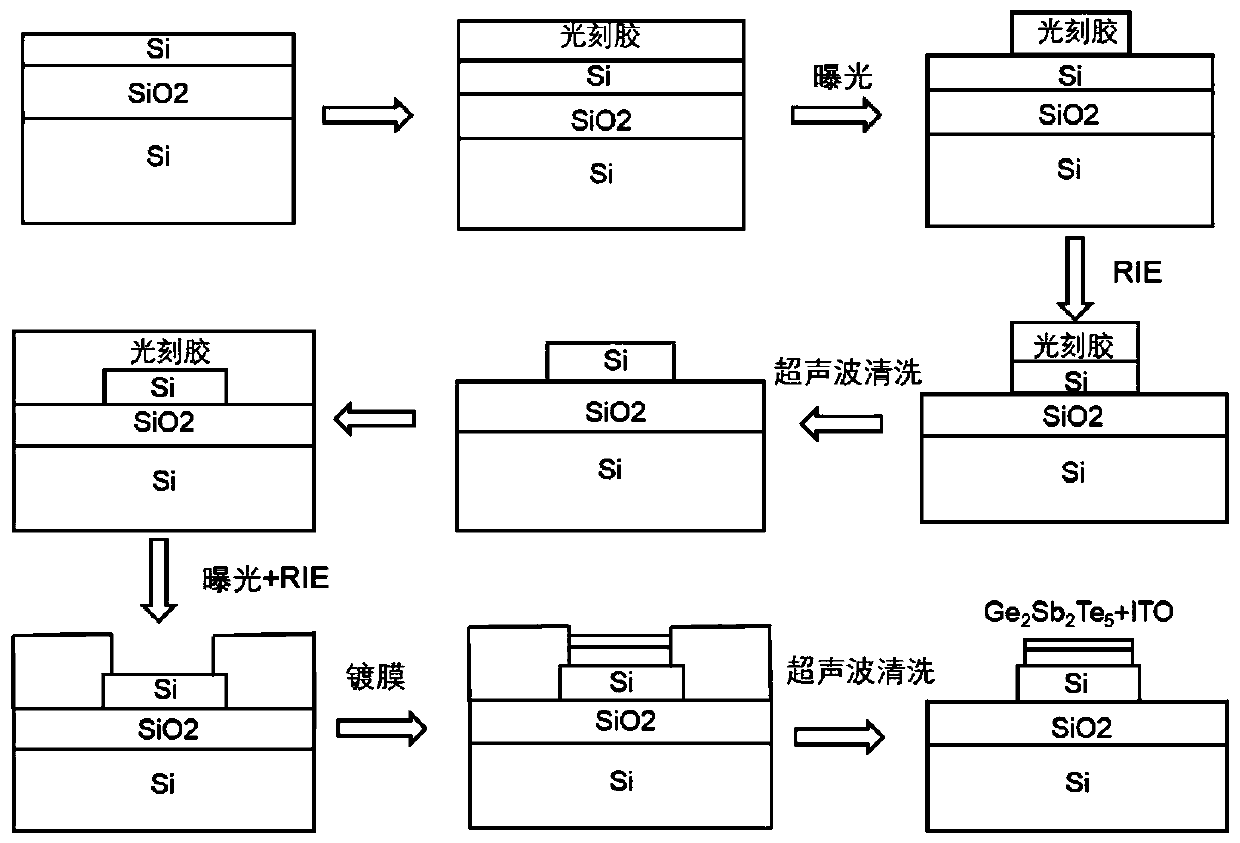
[0036] Step 1, spin-coat the SOI substrate with electron beam photoresist, perform electron beam exposure, and form a rectangular waveguide and a grating structure at both ends by reactive ion etching;
[0037] Step 2, perform the second spin-coated electron beam photoresist and electron beam exposure, and form Ge by reactive ion etching 2 Sb 2 Te 5 , ITO sputtering window. Using a magnetron sputtering coater, plate 25nm thick Ge on the sputtering window 2 Sb 2 Te 5 and 10nm thick ITO;
[0038] Step 3, the prepared substrate is ultrasonically cleaned with acetone and alcohol in sequence, and then rinsed with deionized water to completely remove the photoresist;
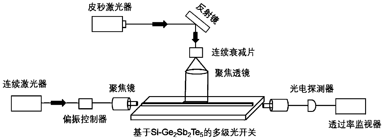
[0039] Step 4, put the prepared substrate into image 3 in the working system;
[0040] Step 5, modulate the external picosecond laser, in the waveguide mixing area Si-Ge 2 Sb 2 Te 5 Focus on the picosecond laser. By adjusting the pumping energy of the laser and the continuous attenuation sheet to adjust t...
PUM
| Property | Measurement | Unit |
|---|---|---|
| Thickness | aaaaa | aaaaa |
| Width | aaaaa | aaaaa |
Abstract
Description
Claims
Application Information