
Organic light-emitting material and organic light-emitting device

A light-emitting material, organic technology, applied in the direction of light-emitting materials, electro-solid devices, electrical components, etc., can solve the problems of mismatch of electrons and holes, poor luminous efficiency, poor injection effect, etc., to reduce the start-up voltage, Good thermodynamic stability, favorable effect of molecular packing

Active Publication Date: 2020-06-12
YANTAI XIANHUA CHEM TECH CO LTD
View PDF10 Cites 9 Cited by
  • Summary
  • Abstract
  • Description
  • Claims
  • Application Information

AI Technical Summary

Problems solved by technology

Currently used phosphorescent host materials often have a single carrier transport capability, such as hole transport hosts and electron transport hosts. However, a single carrier transport capability will cause a mismatch between electrons and holes in the light-emitting layer. , resulting in severe efficiency roll-off and shortened life
[0005] A class of host materials has been reported in CN10563695A9 patent, but due to the problem of energy level matching, the injection effect is not good and the device voltage is high; a similar structure is also reported in CN106255687A, but the luminous efficiency is not good

Method used


Image

  • Organic light-emitting material and organic light-emitting device
  • Organic light-emitting material and organic light-emitting device
  • Organic light-emitting material and organic light-emitting device

Examples


Embodiment 1

[0098] The glass plate coated with the ITO transparent conductive layer is ultrasonically treated in a commercial cleaning agent, rinsed in deionized water, ultrasonically degreased in acetone-ethanol mixed solvent, baked in a clean environment until the water is completely removed, and then cleaned with ultraviolet light. Light and ozone cleaning, and bombardment of the surface with a beam of low-energy cations;

[0099] Place the above-mentioned glass substrate with the anode in a vacuum chamber, and evacuate to less than 10 -5 , HT-11 was vacuum evaporated on the anode layer as a hole injection layer, the evaporation rate was 0.1nm / s, and the evaporation film thickness was 10nm;

[0100] On the hole injection layer, HT-5 material was vacuum evaporated as the hole transport layer, the evaporation rate was 0.1nm / s, and the total film thickness was 80nm;

[0101] The light-emitting layer of the device is vacuum evaporated on the hole transport layer. The light-emitting layer ...

Embodiment 2-6

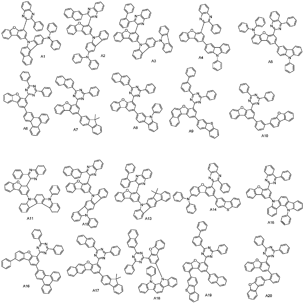
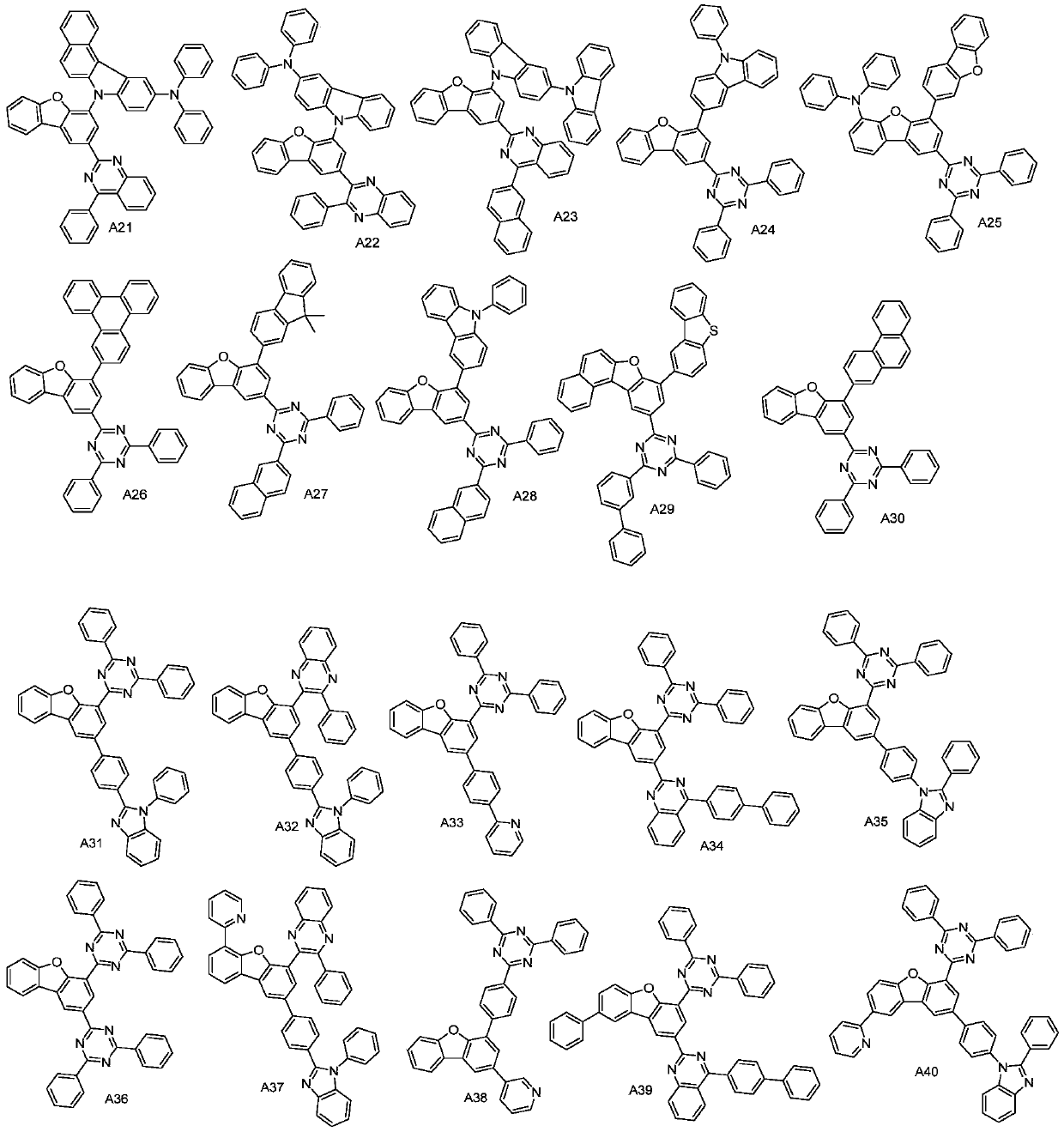
[0107] The organic light-emitting materials A6, A12, A19, A24 and A29 of the present application were respectively used as the host material of the light-emitting layer, and the rest were the same as in Example 1. The test results are shown in Table 1.

Embodiment 7

[0115] The glass plate coated with the ITO transparent conductive layer is ultrasonically treated in a commercial cleaning agent, rinsed in deionized water, ultrasonically degreased in acetone-ethanol mixed solvent, baked in a clean environment until the water is completely removed, and then cleaned with ultraviolet light. Light and ozone cleaning, and bombardment of the surface with a beam of low-energy cations;

[0116] Place the above-mentioned glass substrate with the anode in a vacuum chamber, and evacuate to less than 10 -5 , HT-11 was vacuum evaporated on the anode layer as a hole injection layer, the evaporation rate was 0.1nm / s, and the evaporation film thickness was 10nm;

[0117] On the hole injection layer, HT-5 material was vacuum evaporated as the hole transport layer, the evaporation rate was 0.1nm / s, and the total film thickness was 80nm;

[0118]The light-emitting layer of the device is vacuum-evaporated on the hole transport layer. The light-emitting layer i...


PUM


Abstract

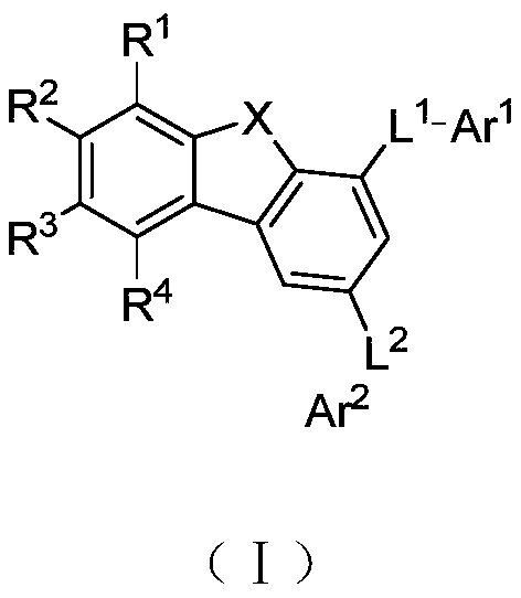
The invention provides a novel organic light-emitting material. The novel organic light-emitting material is used for a light-emitting main body material and an electron transport layer material of anorganic light-emitting device. The invention also provides an organic light-emitting device comprising the novel organic light-emitting material.

Description

technical field [0001] The application relates to a novel organic compound, in particular to an organic luminescent material and an organic electroluminescent device using the organic luminescent material. Background technique [0002] Electroluminescence (EL) refers to the phenomenon that luminescent materials emit light under the action of an electric field and are excited by current and electric field. It is a luminescence process that directly converts electrical energy into light energy. Organic electroluminescent display (hereinafter referred to as OLED) has a series of advantages such as self-luminescence, low-voltage DC drive, full curing, wide viewing angle, light weight, simple composition and process, etc. Compared with liquid crystal display, organic electroluminescent display is not It requires a backlight source, has a large viewing angle and low power, and its response speed can reach 1000 times that of a liquid crystal display, but its manufacturing cost is l...

Claims


Application Information

Patent Timeline
Patent Type & Authority Applications(China)
IPC IPC(8): C07D405/04C07D405/14C07D409/14C07D471/04C07D487/04C09K11/06H01L51/54H01L51/50
CPCC07D405/14C07D405/04C07D409/14C07D487/04C07D471/04C09K11/06C09K2211/1044C09K2211/1059C09K2211/1088C09K2211/1029C09K2211/1092C09K2211/1011H10K85/622H10K85/636H10K85/615H10K85/654H10K85/6576H10K85/6574H10K85/6572H10K50/12H10K50/16
Inventor 邢其锋丰佩川孙志武胡灵峰陈跃陈义丽
Owner YANTAI XIANHUA CHEM TECH CO LTD
Learn More