Single-electron transmission avalanche photodiode structure and manufacturing method

An avalanche photoelectric and diode technology, applied in circuits, electrical components, semiconductor devices, etc., can solve problems such as increased leakage current, damage, and inability to meet device bandwidth and overload optical power at the same time

Active Publication Date: 2020-06-19
THE 44TH INST OF CHINA ELECTRONICS TECH GROUP CORP
View PDF14 Cites 0 Cited by
  • Summary
  • Abstract
  • Description
  • Claims
  • Application Information

AI Technical Summary

Problems solved by technology

[0002] The bandwidth, gain and overload optical power of the avalanche photodiode (APD) device parameters are physical characteristics that are mutually inhibited. The contradiction of power is more prominent; APDs have been developed so far, and they all adopt the absorption, gradual change, charge, and multiplication separation (SAGCM) structure. The traditional SAGCM structure cannot meet the requirements of bandwidth and overload optical power when the device works at high speed.
[0003] In the current InGaAs / InP-based APD structure, electrons and holes are used for carrier transport, and the mobility of holes is lower than that of electrons. It is easy to accumulate at the PN interface or energy band discontinuity, resulting in space charge shielding effect, which limits the device. Frequency (speed) and saturation (overload optical power) characteristics
[0004] In addition, the side wall of the traditional mesa detector device is grown by plasma enhanced chemical vapor deposition (PECVD) silicon dioxide (SiO2), silicon nitride (SiNx) or coated with polyimide (PI), benzocyclobutene (BCB) for passivation, too high process temperature or low medium density will destroy the dangling bonds on the surface of compound semiconductors during plasma bombardment, resulting in unstable surface states and increased leakage current, making it effective in practical applications bad

Method used


Image

  • Single-electron transmission avalanche photodiode structure and manufacturing method
  • Single-electron transmission avalanche photodiode structure and manufacturing method
  • Single-electron transmission avalanche photodiode structure and manufacturing method

Examples


Embodiment 1

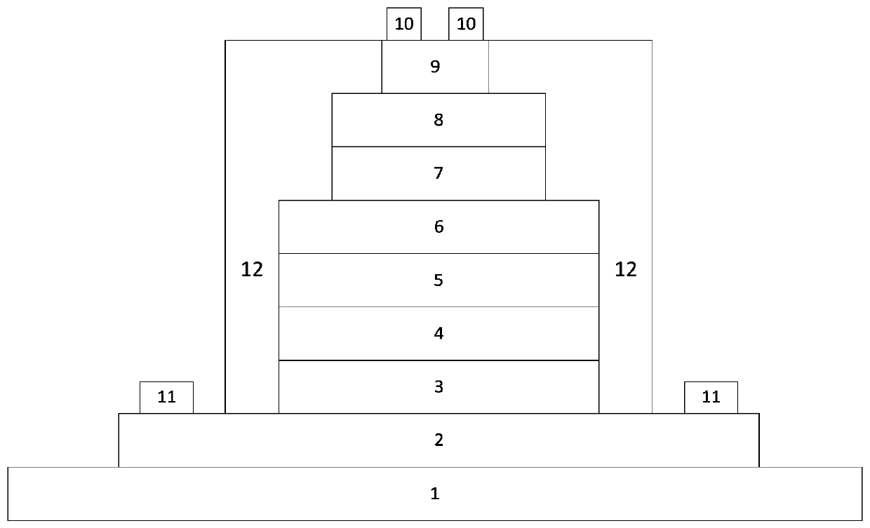
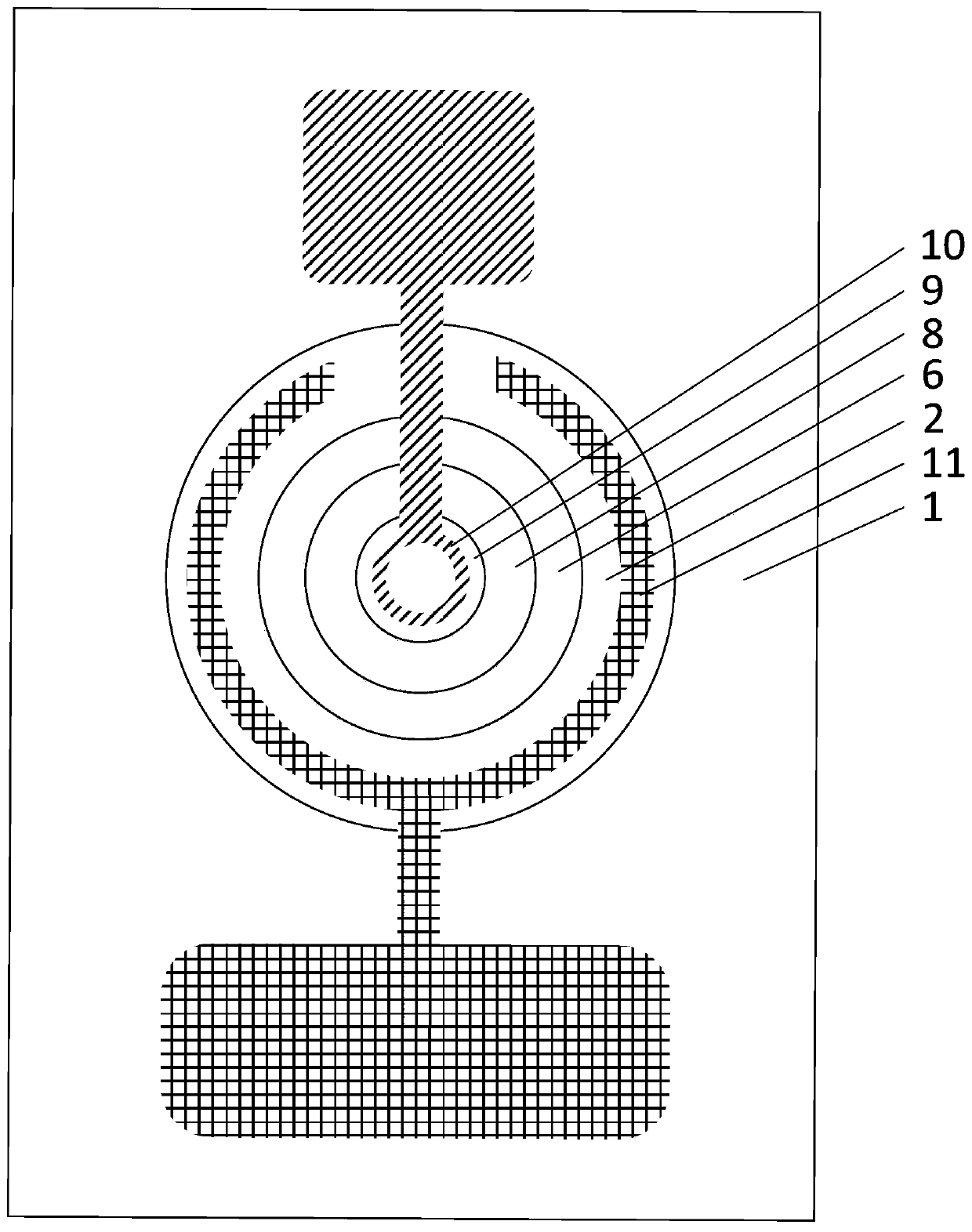
[0045] Such as figure 1 and figure 2 As shown, one embodiment of the single electron transport avalanche photodiode structure of the present invention comprises an InP semi-insulating substrate 1, on which a P-type InAlGaAs contact layer 2, a P-type InAlGaAs contact layer 2, and a P-type In 0.53 Ga 0.47 As absorption layer 3, unintentionally doped InGaAlAs graded layer 4, P-type In 0.52 al 0.48 As field control layer 5, unintentionally doped In 0.52 al 0.48 As multiplication layer 6, N-type In 0.52 al 0.48 As field control layer 7, N-type In 0.52 al 0.48 As buffer layer 8 and N-type In 0.53 Ga 0.47 As contact layer 9; the N-type In 0.53 Ga 0.47 The As contact layer 9 is connected to an N-type electrode 10 , and the P-type InAlGaAs contact layer 2 is connected to a P-type electrode 11 .

[0046] The photodiode structure is a concentric circular structure with four layers of mesas, and the first layer of mesas is N-type In 0.53 Ga 0.47 The upper surface of the As...

Embodiment 2

[0070] Such as Figure 4 and Figure 5 As shown, another embodiment of the single electron transport avalanche photodiode structure of the present invention includes an InP semi-insulating substrate 1', and N-type In is grown sequentially on the InP semi-insulating substrate 1'. 0.52 al 0.48 As contact layer 9', unintentionally doped In 0.52 al 0.48 As multiplication layer 6', P-type In 0.52 al 0.48 As field control layer 5', unintentionally doped InGaAlAs graded layer 4', P-type In 0.53 Ga 0.47 As absorption layer 3' and P-type In 0.53 Ga 0.47 As contact layer 20, the P-type In 0.53 Ga 0.47 The As contact layer 20 is connected with a P-type electrode 11', and the N-type In 0.52 al 0.48 The As contact layer 9' is connected to an N-type electrode 10'.

[0071] The photodiode structure is a concentric circular structure with three layers of mesas, and the first layer of mesas is P-type In 0.53 Ga 0.47 The upper surface of the As contact layer 20, the second mesa i...


PUM

PropertyMeasurementUnit
thicknessaaaaaaaaaa
thicknessaaaaaaaaaa
thicknessaaaaaaaaaa

Abstract

The invention discloses a single-electron transmission avalanche photodiode structure including a substrate, a P-type InAlGaAs contact layer, a P-type InGaAs absorption layer, an unintentionally dopedInGaAlAs gradient layer, a P-type InAlAs field control layer, an unintentionally doped InAlAs multiplication layer, an N-type InAlAs field control layer, an N-type InAlAs buffer layer and an N-type InGaAs contact layer are grown on the substrate in sequence. The invention also discloses a manufacturing method of the single-electron transmission avalanche photodiode structure, another single-electron transmission avalanche photodiode structure and a manufacturing method thereof. According to the invention, the InGaAs absorption layer is designed to be P-type doped, photo-generated holes are majority carriers, the photo-generated holes participate in carrier transmission in a relaxation process, only electrons are generated in carrier migration, and the frequency and saturation characteristics of a device are greatly improved through the electrons with high mobility.

Description

technical field [0001] The invention relates to the field of semiconductor devices, in particular to a single-electron transport avalanche photodiode structure and a manufacturing method. Background technique [0002] The bandwidth, gain and overload optical power of the avalanche photodiode (APD) device parameters are physical characteristics that inhibit each other. The contradiction of power is more prominent; APDs have adopted absorption, gradual change, charge, multiplication separation (SAGCM) structure since the development, and the traditional SAGCM structure cannot meet the requirements of bandwidth and overload optical power when the device works at high speed. [0003] In the current InGaAs / InP-based APD structure, electrons and holes are used for carrier transport, and the mobility of holes is lower than that of electrons. It is easy to accumulate at the PN interface or energy band discontinuity, resulting in space charge shielding effect, which limits the device...

Claims


Application Information

Patent Timeline
Patent Type & Authority Applications(China)
IPC IPC(8): H01L31/0352H01L31/0304H01L31/107H01L31/18
CPCH01L31/035272H01L31/035281H01L31/1868H01L31/1075H01L31/1844H01L31/03046H01L31/03042Y02P70/50
Inventor 黄晓峰张承王立唐艳高新江莫才平
Owner THE 44TH INST OF CHINA ELECTRONICS TECH GROUP CORP
Why Eureka
Try Eureka