Silicon carbide MOSFET and preparation method thereof

A technology of silicon carbide and silicon carbide substrates, applied in semiconductor/solid-state device manufacturing, semiconductor devices, electrical components, etc., can solve problems such as increasing field strength, SiC MOSFET needs to be improved, and low electron mobility in the inversion layer

Active Publication Date: 2020-06-23
BYD CO LTD
View PDF6 Cites 1 Cited by
  • Summary
  • Abstract
  • Description
  • Claims
  • Application Information

AI Technical Summary

Problems solved by technology

Although it has the above advantages, the electric field concentration effect increases the field strength at the bottom corner of the trench, and the field strength of the gate oxide layer at the MOS interface has exceeded the semiconductor electric field strength, which may cause the gate oxide layer to break down before the PN junction, so Its maximum blocking voltage is limited by the breakdown of the gate oxide layer rather than by the breakdown of the semiconductor; in addition, the electron mobility of the inversion layer is small, especially on the side wall of the trench, so the characteristic on-resistance is large
[0003] Therefore, the current SiC MOSFET still needs to be improved

Method used


Image

  • Silicon carbide MOSFET and preparation method thereof
  • Silicon carbide MOSFET and preparation method thereof
  • Silicon carbide MOSFET and preparation method thereof

Examples


Embodiment 1

[0049] Preparation methods include:

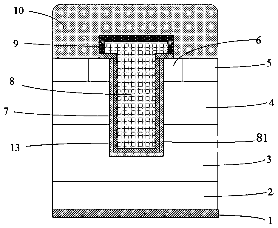
[0050] Step 1: On the heavily doped n+ type SIC substrate 2, the first epitaxial layer 31 of n-type SIC is epitaxially formed by PECVD; the doping concentration of the first epitaxial layer 31 is 1×10 15 cm -3 , the thickness is 10 microns, the doping impurity is nitrogen (N), and the structural diagram is shown in Figure 5 .

[0051] Step 2: Etching the n-type first epitaxial layer 31 to form a step profile, the etching depth is 0.1 micron, see the structure schematic diagram Figure 6 .

[0052] Step 3: Epitaxially form a heavily doped p+ epitaxial layer 121 on the etched n-type first epitaxial layer 31 and perform etching to form the p+ heavily doped region 12; the p+ heavily doped region 12 The doping concentration is 1×10 16 cm -3 , the doping impurity is aluminum (Al), and the thickness is 1 micron; Figure 7 , Figure 8 shown.

[0053] Step 4: Continue epitaxially forming an n-lightly doped second epitaxial layer 32 on the...

Embodiment 2

[0062] Preparation methods include:

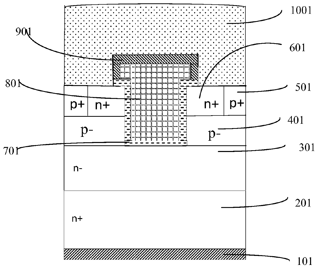
[0063] Step 1: On the heavily doped n+ type SIC substrate 2, an n-type SIC epitaxial layer 3 is formed by MOCVD epitaxy; the doping concentration of the epitaxial layer 3 is 5×10 15 cm -3 , the thickness is 15 microns, the dopant impurity is nitrogen (N), and the structural diagram is shown in Figure 4 .

[0064] Step 2: Epitaxially form a p-type epitaxial layer 4 on the n-type epitaxial layer 3; the doping concentration of the p-type SIC lightly doped epitaxial layer 4 is 5×10 13 cm -3 , the doping impurity is aluminum (Al), and the thickness is 2.5 microns; if Figure 4 shown;

[0065] Step 3: forming n+ source region 6 and p+ contact region 5 on epitaxial layer 4 by photolithography and implantation; the doping concentration of source region 6 is 1×10 15 cm -3 , the doping concentration of the contact region 5 is 5×10 15 cm -3 ; and carry out high temperature annealing after implantation, the annealing temperature is between 1...

Embodiment 3

[0072] Preparation methods include:

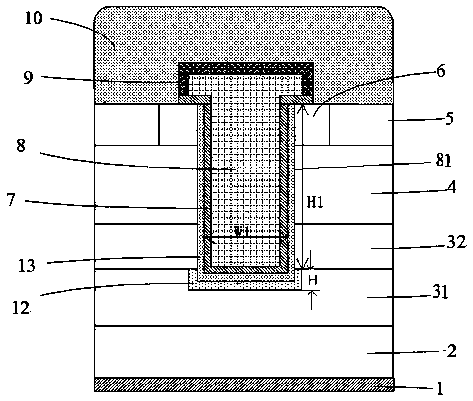
[0073] Step 1: On the heavily doped n+ type SIC substrate 2, the first epitaxial layer 31 of n-type SIC is epitaxially formed by PECVD; the doping concentration of the first epitaxial layer 31 is 1×10 16 cm -3 , the thickness is 15 microns, the dopant impurity is nitrogen (N), and the structural diagram is shown in Figure 5 .

[0074] Step 2: Etching the n-type first epitaxial layer 31 to form a step profile, the etching depth is 0.4 microns, see the structure schematic diagram Figure 6 .

[0075] Step 3: Epitaxially form a heavily doped p+ epitaxial layer 121 on the etched n-type first epitaxial layer 31 and perform etching to form the p+ heavily doped region 12; the p+ heavily doped region 12 The doping concentration is 1×10 17 cm -3 , the doping impurity is aluminum (Al), and the thickness is 2 microns; as Figure 7 , Figure 8 shown.

[0076] Step 4: Continue epitaxially forming an n-lightly doped second epitaxial layer 32 o...


PUM

PropertyMeasurementUnit
thicknessaaaaaaaaaa
thicknessaaaaaaaaaa
thicknessaaaaaaaaaa

Abstract

The invention provides a silicon carbide MOSFET and a preparation method thereof. The silicon carbide MOSFET comprises a silicon carbide substrate, a first conductive type lightly doped epitaxial layer, a second conductive type lightly doped epitaxial layer, a contact region, a source region, a gate groove, a lightly doped injection region, a gate oxide layer, a gate, a dielectric layer, a metal electrode and a drain. According to the silicon carbide MOSFET, the first conductive type lightly doped injection region is arranged on the inner wall of the gate groove, so that the carrier concentration of a channel surface region can be effectively increased, the channel mobility is effectively improved, and the channel resistance is reduced.

Description

technical field [0001] The invention relates to the technical field of semiconductor devices, in particular to a silicon carbide MOSFET and a preparation method thereof. Background technique [0002] The third-generation semiconductor material silicon carbide (SiC) has the characteristics of wide bandgap, high critical breakdown electric field, and high saturation drift rate, and can work well in extreme scenarios such as high temperature, high frequency, and high power, and can further provide Various applications and systems bring significant performance improvements. Among SiC power devices, SiC MOSFET has the advantages of high input impedance, high switching speed stability, and low on-resistance, and is the most concerned SiC switching device. refer to figure 1 , the existing trench SiC MOSFET, epitaxially formed n-SiC drift layer 3 on heavily doped n+SiC substrate 2, formed p-well 4 by implantation on n-drift layer 3, through photolithography and Implant to form so...

Claims


Application Information

Patent Timeline
Patent Type & Authority Applications(China)
IPC IPC(8): H01L29/78H01L29/06H01L21/336
CPCH01L29/7828H01L29/0684H01L29/66068
Inventor 李俊俏李永辉周维
Owner BYD CO LTD
Why Eureka
Try Eureka