Photovoltaic module panel, preparation method thereof and photovoltaic module
A technology of photovoltaic modules and plates, applied in photovoltaic power generation, electrical components, semiconductor devices, etc., can solve the problems of high cost, affecting the barrier and packaging performance of plates, etc., to achieve thinner thickness, meet environmental erosion resistance, and firm combination Effect
- Summary
- Abstract
- Description
- Claims
- Application Information
AI Technical Summary
Problems solved by technology
Method used
Image
Examples
Embodiment 1
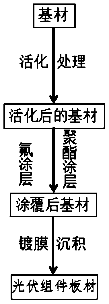
[0049] This embodiment provides a photovoltaic module plate, which includes, from top to bottom: a fluorine coating, a PET substrate, a polyester coating and a barrier layer, where the barrier layer is an inorganic barrier layer.
[0050] The specific preparation method of the photovoltaic module plate comprises the following steps:
[0051] (1) Select a PET substrate with a thickness of 100 μm, and use argon plasma and oxygen plasma to perform plasma corona treatment on the front and back sides under the condition of a vacuum of 2000 Pa, and finally make the surface tension reach 58 dyn / cm;
[0052] (2) A polytetrafluoroethylene coating is formed on the front side of the activated PET substrate through a roll-to-roll coating process, and after drying and aging at 110° C., a fluorine coating with a thickness of 1 μm is obtained.
[0053] (3) Coating a polyacrylic resin coating with a thickness of 50 nm on the reverse side of the fluorine-coated PET substrate.
[0054] (4) The A...
Embodiment 2
[0056] This embodiment provides a photovoltaic module board, which includes, from top to bottom: a fluorine coating, a PEN substrate, a polyester coating and a barrier layer, and the barrier layer is composed of an inorganic-organic barrier layer.
[0057] The specific preparation method of the photovoltaic module plate comprises the following steps:
[0058] (1) Select a PEN base material with a thickness of 120 μm, and perform plasma corona treatment on the front and back sides of the substrate under a vacuum of 1800 Pa by argon plasma and oxygen plasma, so that the surface tension reaches 58 dyn / cm;
[0059] (2) A polyvinylidene fluoride resin coating is formed on the front side of the activated PEN substrate through a roll-to-roll coating process, and after drying and curing at 120° C., a fluorine coating with a thickness of 100 nm is obtained.
[0060] (3) Coating a polyacrylic resin coating with a thickness of 50 nm on the opposite side of the fluorine-coated PEN substra...
Embodiment 3
[0063] This embodiment provides a photovoltaic module plate, which includes: a fluorine coating, a PET substrate, a polyester coating and a barrier layer from top to bottom, and the barrier layer is an inorganic-organic barrier layer.
[0064] The specific preparation method of the photovoltaic module plate comprises the following steps:
[0065] (1) Select a PET base material with a thickness of 120 μm, and perform plasma surface grafting treatment on both sides of the PET substrate. The specific treatment conditions are: the grafting monomer is NH 3 , using DBD dielectric barrier discharge treatment, using Ar plasma to participate in the reaction, so that the surface of the PET substrate produces directional amino active groups, and finally makes the surface tension reach 60dyn / cm;
[0066] (2) A polyvinylidene fluoride resin coating is formed on the front side of the activated PET substrate through a plane coating process, and after drying and curing at 110° C., a fluorine ...
PUM
| Property | Measurement | Unit |
|---|---|---|
| surface tension | aaaaa | aaaaa |
| thickness | aaaaa | aaaaa |
| thickness | aaaaa | aaaaa |
Abstract
Description
Claims
Application Information

