

Method for additive manufacturing of glass substrate PCB and LED display
A glass substrate, PCB board technology, applied in the direction of printed circuit components, metal pattern materials, electrical components to assemble printed circuits, etc., can solve problems such as very high yield challenges, circuit short circuits, and silver paste technology losing cost advantages, etc. Achieve low cost, prevent oxidation, and improve reliability
- Summary
- Abstract
- Description
- Claims
- Application Information
AI Technical Summary
Problems solved by technology
Method used
Image

Examples
Embodiment 1
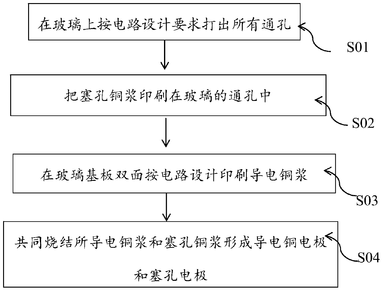
[0046] Double-sided glass substrate PCB board manufacturing, such as figure 1 As shown, the high insulation and high thermal stability of glass can make use of copper paste technology to manufacture double-sided glass substrates and additively manufacture PCB boards.
[0047] A method for manufacturing a double-sided glass substrate PCB board, comprising the steps of:
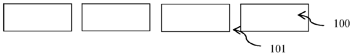
[0048] S01: Drill all through holes 101 on the glass 100 according to circuit design requirements. Such as Figure 1A As shown, the thickness of the glass substrate 100 is 0.1-1 mm. Laser drilling or mechanical drilling is a commonly used glass drilling technology. A picosecond ultraviolet laser can be used to drill through holes 101 with a diameter of 0.05-0.2 mm in the glass 100 . Here, laser and chemical etching can also be combined to create finer through holes without microcracks.
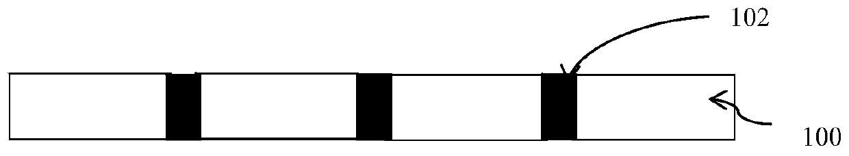
[0049] S02: Print the plug copper paste 102 in the through hole 101 of the glass by using the vacuum plug technology. Su...
Embodiment 2
[0058] Embodiment 2 of the present invention uses printing technology to alternately print conductive paste and insulating dielectric paste, additively manufacture multilayer circuits, and manufacture printed circuits for LED passive driving display on glass substrates.
[0059] A method for manufacturing an additive glass substrate PCB board, such as figure 2 shown, including the following steps:
[0060] S01: Print conductive copper paste on the glass substrate 200, such as Figure 2A shown. In the present invention, copper paste is printed, and the positive electrode copper paste 201 and the negative electrode copper paste 202 (corresponding to X and Y drive electrodes) of the LED are first printed in this step, and the distance between the electrodes is determined according to the size of the LED. For Mini - For LEDs, the electrode spacing can be less than 50 μm. The copper paste in the present invention can print the line width and line spacing below 50 μm, and the li...
Embodiment 3
[0069] Active display generally requires the use of thin film transistors (TFT) to control the light emission and luminous intensity of each LED. The TFT on the glass substrate can be low-temperature amorphous silicon TFT or polysilicon TFT, or indium gallium zinc oxide (IGZO) thin film TFT, the entire array of these TFTs can be manufactured on a glass substrate first, and then laminated and printed with control and drive circuits to form an active display PCB.
[0070] A kind of manufacturing method of additive manufacturing glass substrate PCB board, such as image 3 shown, including the following steps:
[0071] S01: Fabricate a TFT array 301 on a glass substrate, such as Figure 3A . The TFT may be a low-temperature amorphous silicon TFT or polysilicon TFT, or may be an indium gallium zinc oxide (IGZO) thin film TFT.
[0072] S02: Print the conductive copper paste 302 connected to the TFT array, such as Figure 3B As shown, the gray in the figure is the conductive copp...
PUM
| Property | Measurement | Unit |
|---|---|---|
| Thickness | aaaaa | aaaaa |
| Softening point | aaaaa | aaaaa |
| Thermal expansion coefficient | aaaaa | aaaaa |
Abstract
Description
Claims
Application Information