Adjustable light delay line of silicon-based coupling waveguide and method for regulating and controlling light delay

A technology of coupling waveguide and delay line, which is applied in the field of adjustable optical delay line and optical delay of silicon-based coupled waveguide, can solve the problems of high cost, difficult to realize, complicated experimental system, etc. Time and time, the effect of large bandwidth

Active Publication Date: 2020-07-10
CHINA JILIANG UNIV
View PDF8 Cites 2 Cited by
  • Summary
  • Abstract
  • Description
  • Claims
  • Application Information

AI Technical Summary

Problems solved by technology

However, the EIT technology uses the quantum coherence effect to eliminate the influence of the medium in the process of electromagnetic wave propagation. The experimental system is complex, the cost is expensive, and it is difficult to realize at room temperature.

Method used


Image

  • Adjustable light delay line of silicon-based coupling waveguide and method for regulating and controlling light delay
  • Adjustable light delay line of silicon-based coupling waveguide and method for regulating and controlling light delay
  • Adjustable light delay line of silicon-based coupling waveguide and method for regulating and controlling light delay

Examples


Embodiment Construction

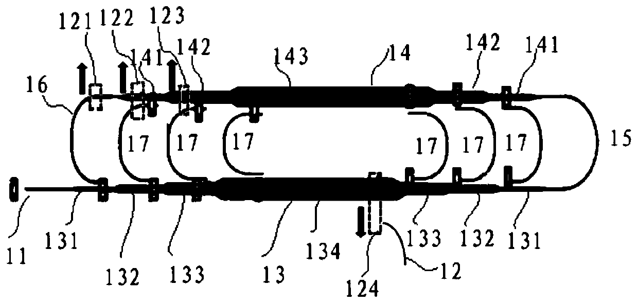
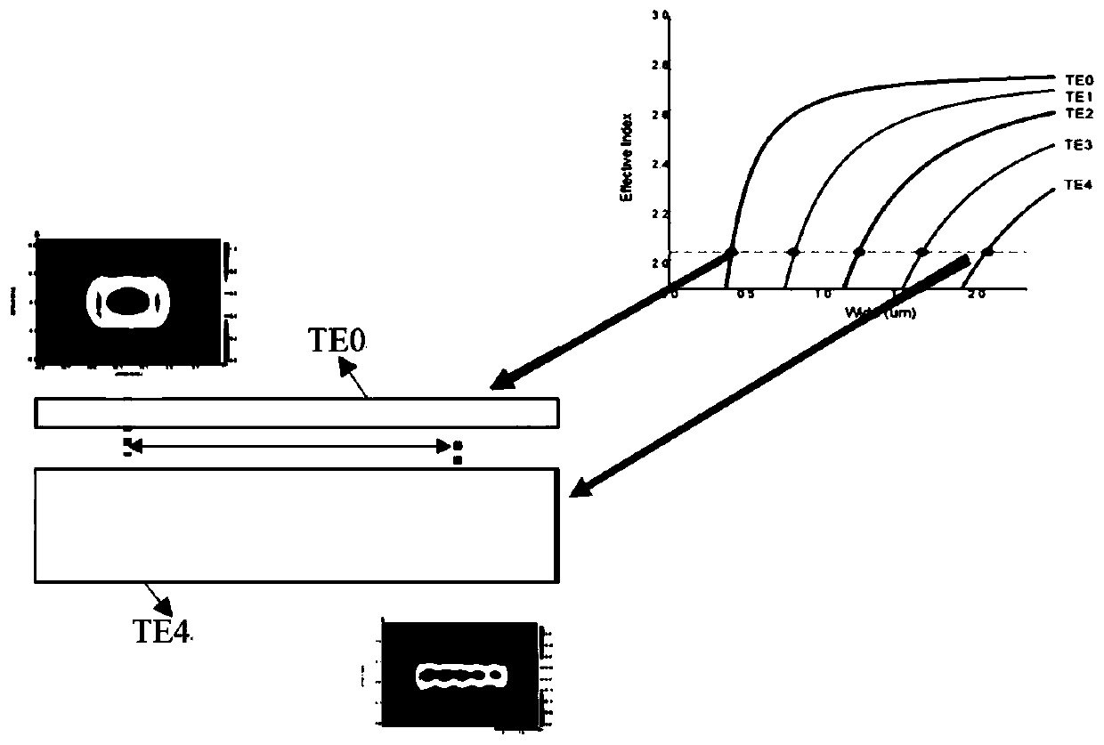
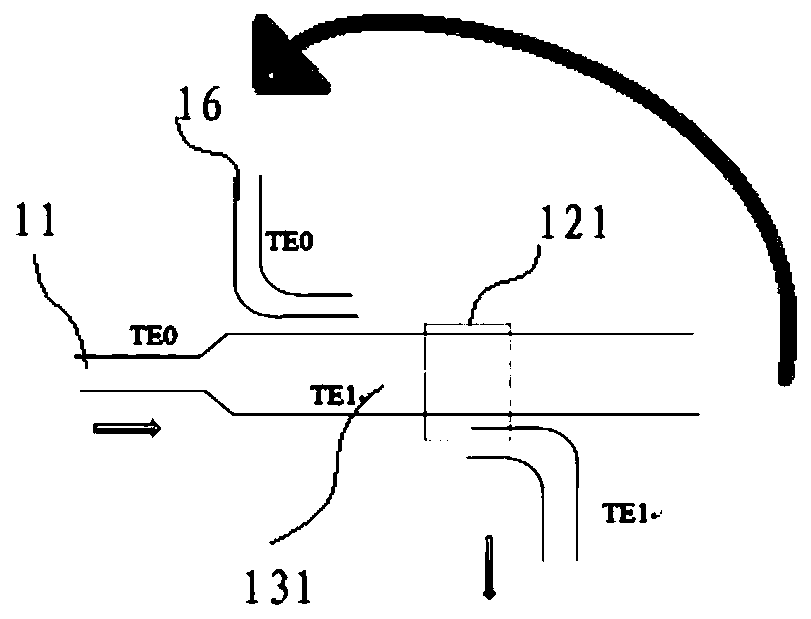
[0023] For ease of understanding, the technical principle of the present invention will be described below first. See figure 2 and image 3 , figure 2 It is a schematic diagram of optical signal jumping between two different waveguides based on the principle of coupled waves. As shown in the figure, the principle of coupled waves is that energy is transferred from one waveguide to another waveguide. In a continuous waveguide, optical signals in different modes, such as from TE0 mode to TE4 mode, energy is transmitted from one part of the waveguide to another part, and the energy of one mode is converted into the energy of another mode. However, when two optical waveguides with different dispersion curves intersect at the phase-matched wavelength node, that is, when the mode-field matching and the effective refractive index are both satisfied, the coupling can only be performed when they are close to each other. figure 2 The coordinate diagram in the upper right part is ...


PUM

PropertyMeasurementUnit
sizeaaaaaaaaaa

Abstract

The invention discloses an adjustable light delay line of a silicon-based coupling waveguide. The adjustable light delay line comprises a runway type silicon waveguide structure, an input waveguide, an output waveguide and a delay regulation and control part which are arranged on the upper surface of an SOI substrate. If the phases are matched, the energy exchange can reach 99.9% in two parallel and adjacent coupling waveguides with the same parameters and almost no loss according to the coupling wave principle. After the two waveguides are coupled with each other, the optical signal can be continuously transmitted in the multi-ring runway type structure, thereby generating an optical delay effect. Regulation and control of light delay time are realized by utilizing the characteristics ofthe phase-change material GST. The adjustable light delay line can still enable the output bandwidth to be large on the premise that the structure is compact, and integration is better facilitated; the loss is only 2.96 dB, the delay time reaches 58.8 ps, multi-stage regulation and control can be achieved according to requirements and the overall size is only 0.006 mm < 2 >.

Description

technical field [0001] The invention belongs to the field of silicon-based photonics, and in particular relates to a silicon-based coupling waveguide adjustable optical delay line and an optical delay method. Background technique [0002] Silicon-based photonic devices are research hotspots in recent years, and the delay of optical signals is a basic function in time-domain optical signal processing. Photons cannot be stored, so optical buffering is achieved by delaying the optical signal for a period of time in a light-guiding medium. "Optical cache" can start from two aspects: one is to slow down the propagation speed of light; the other is to extend the optical transmission path. There are two types of all-optical buffers currently proposed: one is slow-optical all-optical buffers; the other is optical fiber delay line or optical fiber ring all-optical buffers. The EIT technology uses the quantum coherence effect to eliminate the influence of the medium in the process o...

Claims


Application Information

Patent Timeline
Patent Type & Authority Applications(China)
IPC IPC(8): G02B6/28
CPCG02B6/2861
Inventor 郝然李伊凡金尚忠石岩
Owner CHINA JILIANG UNIV
Why Eureka
Try Eureka