Silicon heterojunction solar cell comprising silicon nitride antireflection layer and preparation method of layer

A silicon nitride reduction and silicon heterojunction technology, applied in the direction of circuits, photovoltaic power generation, electrical components, etc., can solve the problems affecting the anti-reflection effect and low refractive index, so as to improve the photocurrent, reduce light reflection, and reduce reflection Effect

Inactive Publication Date: 2020-07-14
熵熠(上海)能源科技有限公司
View PDF8 Cites 0 Cited by
  • Summary
  • Abstract
  • Description
  • Claims
  • Application Information

AI Technical Summary

Problems solved by technology

If a high transmittance of the TCO layer is required, it will inevitably lead to a low refractive index, and the low r

Method used


Image

  • Silicon heterojunction solar cell comprising silicon nitride antireflection layer and preparation method of layer

Examples


Example Embodiment

[0026] Example 1

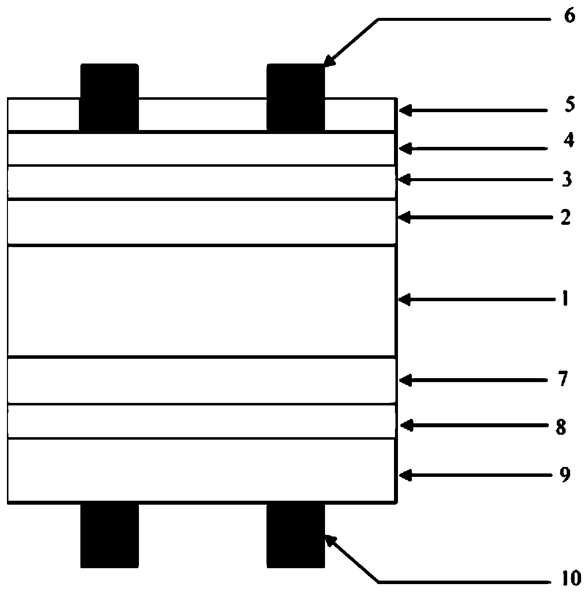
[0027] A method for preparing a silicon heterojunction solar cell containing a silicon nitride anti-reflection layer:

[0028] Step 1: Prepare n-type monocrystalline silicon wafers with industrial grade crystal orientation of (100), resistivity of 0.5-3Ω·cm, and thickness of 100-180μm n-type Cz monocrystalline silicon wafers as substrates, using potassium hydroxide solution Remove the surface damage layer formed by wire cutting;

[0029] Step 2: Use an alkaline solution to texturize the substrate obtained in step 1, and then perform standard RCA cleaning to obtain a pretreated silicon wafer;

[0030] Step 3: Put the silicon wafer obtained in step 2 into the vacuum chamber of PECVD, and the background vacuum in the vacuum chamber reaches 5×10 -4 After Pa, under the condition of silicon wafer substrate temperature 150~300℃, use H 2 And SiH 4 It is a reactive gas, the deposition pressure is 10-300Pa, and a layer of intrinsic amorphous film is grown on the front and bac...


PUM

PropertyMeasurementUnit
Thicknessaaaaaaaaaa
Thicknessaaaaaaaaaa
Thicknessaaaaaaaaaa

Abstract

The invention discloses a silicon heterojunction solar cell comprising a silicon nitride antireflection layer and a preparation method. According to the solar cell, an n-type monocrystalline silicon wafer is used as a substrate; an amorphous silicon intrinsic layer, a p-type amorphous silicon emitter layer, a transparent conductive oxide dielectric layer, the silicon nitride antireflection layer and a metal grid line electrode are arranged on the front surface of the substrate; and an amorphous silicon intrinsic layer, an n-type amorphous silicon back electric field layer, a transparent conductive oxide dielectric layer and a metal grid line electrode are arranged on the back surface of the substrate. The preparation method comprises the following steps of: depositing an amorphous siliconintrinsic layer and a p-type amorphous silicon emitter layer/n-type amorphous silicon back electric field layer on the front/back surface of the substrate; depositing a transparent conductive oxide dielectric layer; depositing a silicon nitride antireflection layer; performing laser grooving; screen-printing silver paste; and sintering. According to the silicon heterojunction solar cell and the preparation method thereof of the invention, the transmission and reflection of light can be balanced, the reflection of incident light can be reduced as much as possible, more optical refraction can berealized and transmitted into the cell, photocurrent is improved, and the conversion efficiency of the heterojunction cell is improved.

Description

technical field [0001] The invention relates to a silicon heterojunction solar cell comprising a silicon nitride anti-reflection layer and a preparation method thereof, belonging to the technical field of silicon solar cells. Background technique [0002] Silicon heterojunction solar cells have attracted more and more attention because of their advantages such as high conversion efficiency and fewer process steps. The structure of a general heterojunction cell is that on the front side of an n-type single crystal silicon wafer, from inside to outside, there are intrinsic amorphous silicon thin film layer, p-type amorphous silicon thin film layer, transparent conductive oxide thin film layer (TCO) and the front side. Electrode; the back side is an intrinsic amorphous thin film layer, an n-type amorphous silicon thin film layer, TCO and a back electrode in sequence from the inside to the outside. The TCO layer on the front here is responsible for the function of conducting ca...

Claims


Application Information

Patent Timeline
IPC IPC(8): H01L31/0747H01L31/0216H01L31/0224H01L31/18
CPCH01L31/0747H01L31/02168H01L31/022466H01L31/022475H01L31/18Y02E10/50Y02P70/50
Inventor 刘超李正平杨杰任栋樑陈昌明徐小娜周国平
Owner 熵熠(上海)能源科技有限公司
Why Eureka
Try Eureka