Magnetic nanocrystalline flaky absorbing agent and preparation method thereof

A magnetic nano-absorbent technology, applied in the field of wave-absorbing materials, can solve the problems of increased internal demagnetization field, deterioration of wave-absorbing performance of sheet-shaped absorbing composite materials, and reduction of initial magnetic permeability, achieving less internal defects and microstructure Strong control ability and the effect of improving microwave permeability

Active Publication Date: 2020-07-17
WUHAN UNIV OF TECH
View PDF8 Cites 1 Cited by
  • Summary
  • Abstract
  • Description
  • Claims
  • Application Information

AI Technical Summary

Problems solved by technology

The magnetic film prepared by the magnetron sputtering method is easy to form a columnar crystal structure. When the thickness of the sputtered magnetic layer increases, the crystal grains increase accordingly, and the internal demagnetization field increases to reduce its initial magnetic permeability. The absorbing performance of composite materials will deteriorate

Method used


Image

  • Magnetic nanocrystalline flaky absorbing agent and preparation method thereof
  • Magnetic nanocrystalline flaky absorbing agent and preparation method thereof
  • Magnetic nanocrystalline flaky absorbing agent and preparation method thereof

Examples


Embodiment 1

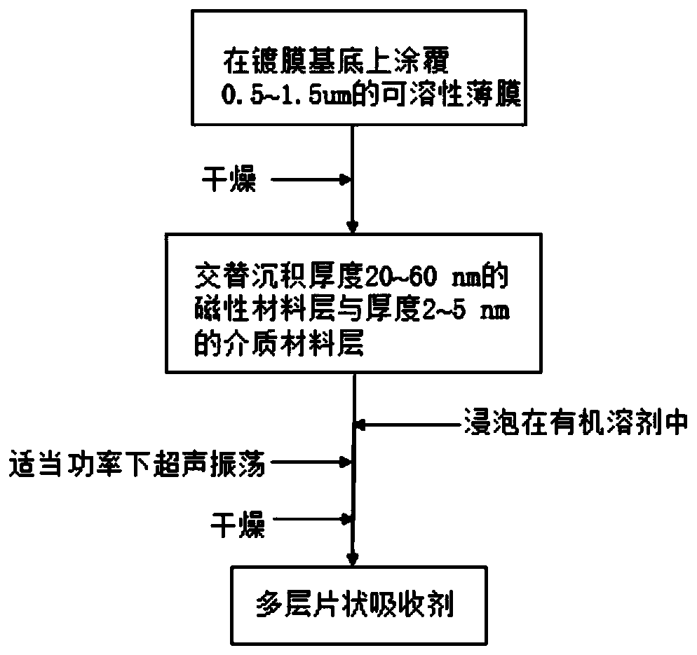
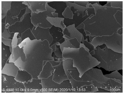
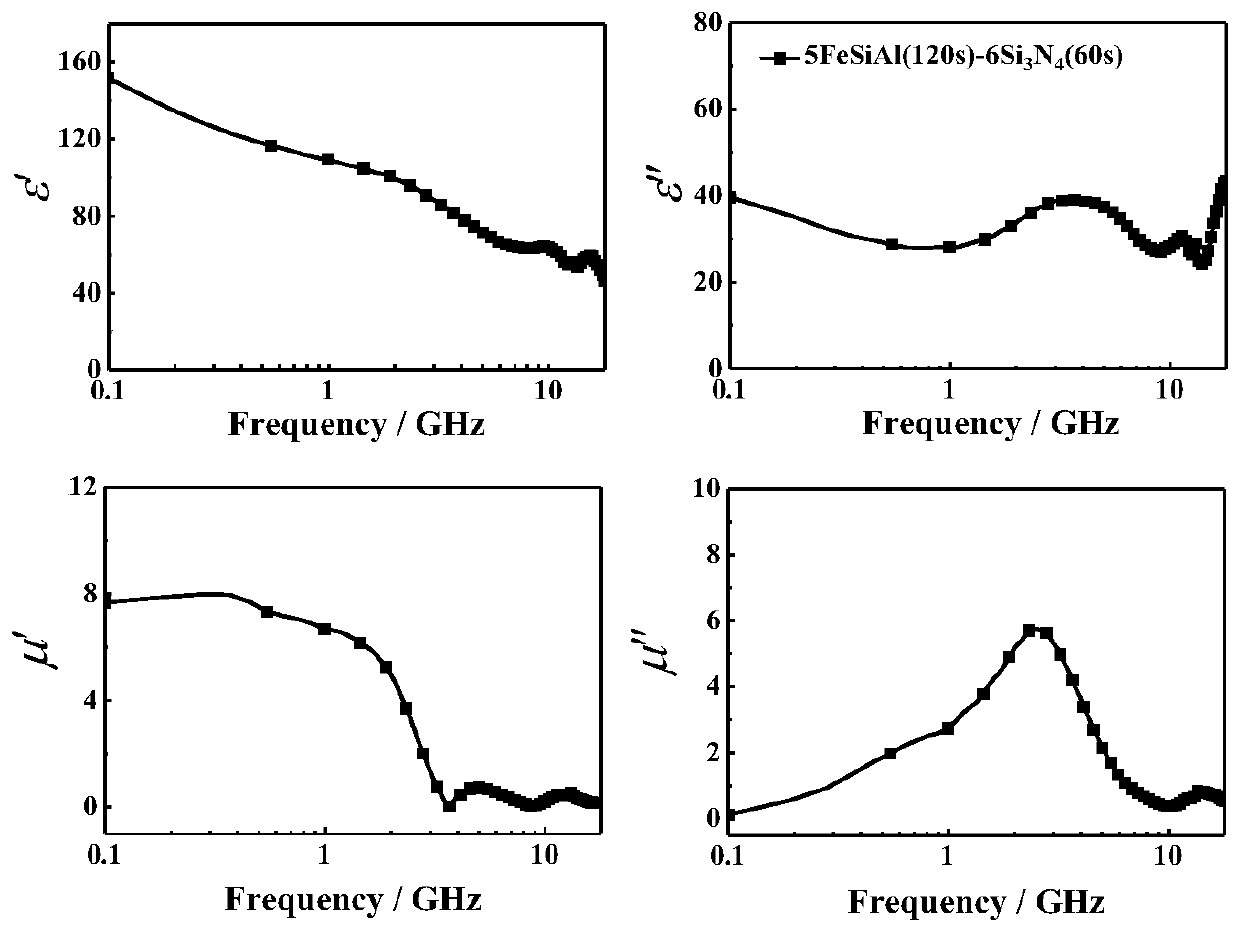
[0039] A solution with a mass ratio of PVP to absolute ethanol of 15% was prepared, and the solution was spin-coated on a glass fiber plate by a spin coater, and the thickness of the coating film was controlled to be 1 μm after drying. Magnetron sputtering was used to alternately sputter FeSiAl magnetic material layers and Si on the glass fiber plate coated with PVP film. 3 N 4 Dielectric material layer, a total of 5 magnetic layers sputtered, 6 dielectric layers, the bottom layer and the top layer are Si 3 N 4 . The sputtering current of FeSiAl target is 0.8A, the sputtering time of each layer is 120s, Si 3 N 4 The target adopts radio frequency sputtering, the sputtering power is 250W, and the sputtering time of each layer is 60s. The sputtering pressure is 0.25Pa, the flow rate of argon gas is 40 sccm, and the rotational speed of the sample stage is 20 r / min. After the sputtering is completed, place the obtained film in absolute ethanol, and set the ultrasonic power de...

Embodiment 2

[0042] A solution with a mass ratio of PVP to absolute ethanol of 15% was prepared, and the solution was spin-coated on a glass fiber plate by a spin coater, and the thickness of the coating film was controlled to be 1 μm after drying. Alternately sputtering Fe magnetic material layer and SiO on glass fiber board by magnetron sputtering 2 Dielectric material layer, a total of 6 magnetic layers sputtered, 7 dielectric layers, the bottom layer and the top layer are SiO 2 . The sputtering current of Fe target is 0.8A, the sputtering time of each layer is 60s, SiO 2 The target is radio frequency sputtering, the sputtering power is 150W, the sputtering time for each layer is 60s, the sputtering pressure is 0.25Pa, the flow rate of argon gas is 40sccm, and the rotation speed of the chassis is 20r / min. After the sputtering is completed, the obtained film is placed in absolute ethanol, and the power density is 1500W / cm 2 . After the shaking was completed, the obtained particles we...

Embodiment 3

[0045] A solution with a mass ratio of PVP to absolute ethanol of 15% was prepared, and the solution was spin-coated on a glass fiber plate by a spin coater, and the thickness of the coating film after drying was controlled to be 1.5 μm. Alternately sputtering Fe magnetic material layer and SiO on glass fiber board by magnetron sputtering 2 Dielectric material layer, the bottom layer and the top layer are SiO 2 . The sputtering current of Fe target is 0.8A, the sputtering time of each layer is 60s, SiO 2 The target adopts radio frequency sputtering, the sputtering power is 150W, and the sputtering time of each layer is 60s. A total of 20 magnetic layers and 21 dielectric layers are sputtered. The sputtering pressure is 0.25 Pa, the argon gas flow rate is 40 sccm, and the rotation speed of the chassis is 20 r / min. After the sputtering is completed, the obtained film is placed in absolute ethanol, and the power density is 500W / cm 2 . After the shaking was completed, the obt...


PUM

PropertyMeasurementUnit
thicknessaaaaaaaaaa
thicknessaaaaaaaaaa
thicknessaaaaaaaaaa

Abstract

The invention relates to the technical field of wave absorbing materials, in particular to a magnetic wave absorbing agent and a preparation method thereof. The preparation method comprises the stepsof alternately depositing a magnetic material with a certain thickness and a medium material on a substrate uniformly coated with a sacrificial layer by adopting a vacuum coating method to obtain a multilayer film, removing the sacrificial layer to obtain a multilayer magnetic film, and crushing the multilayer magnetic film to obtain the magnetic nanocrystalline flaky absorbing agent. The preparation process is simple and convenient, the adjustment is easy, the prepared magnetic nanocrystalline flaky absorbing agent is smooth in surface, few in internal defect, small in stress and controllablein magnetic component, and the magnetic nanocrystalline flaky absorbing agent has the characteristics of multilayer structure, large width-thickness ratio and good surface insulating property. The magnetic permeability bottleneck caused by rough surface, large internal defects and stress, poor microstructure control capability and limited width-thickness ratio of a magnetic nanocrystalline absorbing agent prepared by an existing ball milling method can be broken through, the microwave permeability of the flaky magnetic absorbing agent suitable for different frequency bands is improved, and the dielectric constant of the flaky magnetic absorbing agent is inhibited.

Description

technical field [0001] The invention relates to the technical field of wave-absorbing materials, in particular to a magnetic wave-absorbing agent and a preparation method thereof. Background technique [0002] Absorbing material is an important dual-use material for both military and civilian use. It has extensive and important applications in the fields of radar stealth of weapons and equipment, electromagnetic compatibility of civilian equipment, and prevention and control of electromagnetic pollution. In most scenarios, absorbing materials are required to have as small a thickness as possible and wider and stronger absorption performance, which is also the focus and difficulty in the field of absorbing materials at present. Under the condition of small thickness, the key to improving the absorbing performance is to increase the magnetic permeability and magnetic loss, so this is the core goal of the present invention. Proper selection of absorbent components is a prerequ...

Claims


Application Information

Patent Timeline
Patent Type & Authority Applications(China)
IPC IPC(8): C23C14/06C23C14/10C23C14/18C23C14/20C23C14/35C23C14/30C23C14/32C23C14/08B02C19/18H05K9/00H01Q17/00
CPCB02C19/18C23C14/0005C23C14/0652C23C14/08C23C14/10C23C14/185C23C14/205C23C14/30C23C14/32C23C14/352H01Q17/00H05K9/0081
Inventor 李维鲍禹官建国刘星陈志宏
Owner WUHAN UNIV OF TECH
Why Eureka
Try Eureka