
A method for constructing a near-infrared self-driven photodetector based on semiconductor nanowires/graphene

A technology of photodetectors and nanowires, which is applied in semiconductor devices, circuits, electrical components, etc., can solve problems that cannot meet people's detection needs and limited near-infrared light response sensitivity, and achieve enhanced self-driving characteristics and light response sensitivity, optimized Interface contact, highly reproducible effect

Active Publication Date: 2022-07-29
SHANGHAI NAT ENG RES CENT FORNANOTECH
View PDF6 Cites 0 Cited by
  • Summary
  • Abstract
  • Description
  • Claims
  • Application Information

AI Technical Summary

Problems solved by technology

The current commercial near-infrared photodetectors still have limitations: silicon-based and InGaAs-based photodetectors work normally at room temperature, but their response sensitivity to near-infrared light is limited, which cannot meet people's detection needs.
[0008] Graphene-based optoelectronic devices are being extensively researched and improved. However, the research and development of graphene-based near-infrared photodetectors with high responsivity, low energy consumption and even self-driving still face great challenges.

Method used


Image

  • A method for constructing a near-infrared self-driven photodetector based on semiconductor nanowires/graphene
  • A method for constructing a near-infrared self-driven photodetector based on semiconductor nanowires/graphene

Examples


Embodiment 1

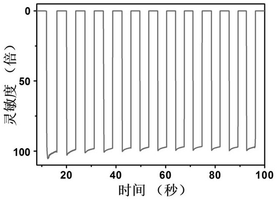
[0026] The graphene film prepared by chemical vapor deposition was transferred to commercial intrinsic Ge to obtain a graphene / Ge sample. Au / Ti electrodes were deposited on the graphene surface of the sample, and then a semiconductor with a concentration of 0.1 mg / mL was deposited. The suspension of semiconducting carbon nanotubes is dripped from a fixed position at one end of the graphene / Ge sample with a pipette (a single drop is 200 μL), so that the suspension liquid of semiconducting carbon nanotubes spreads to the entire graphene / Ge by itself. surface of the sample, and then the sample was dried on a hot plate. After this step is repeated 5 times, the semiconducting carbon nanotube / graphene / Ge sample is placed in a vacuum oven, and after annealing at 60 °C for 20 min, an ideal self-driving performance and sensitivity based on semiconducting carbon nanotube / Ge can be obtained. Near-infrared photodetectors of graphene. attached figure 1 The light response sensitivity-time...

Embodiment 2

[0028] The graphene film prepared by chemical vapor deposition was transferred to a commercial n-type Ge substrate to obtain a graphene / Ge sample, and then the semiconducting carbon nanotube suspension with a concentration of 0.1 mg / mL was pipetted. Dropped from a fixed position at one end of the graphene / Ge sample (a single drop of 200 μL), let the semiconducting carbon nanotube suspension liquid spread to the entire surface of the graphene / Ge sample, and then place the sample on a hot plate Dry on. After this step was repeated 5 times, the semiconducting carbon nanotube / graphene / Ge sample was placed in a vacuum oven, and after annealing at 80 °C for 20 min, Al electrode was evaporated on the carbon nanotube network to obtain self-driving performance. A near-infrared photodetector based on semiconducting carbon nanotubes / graphene with ideal sensitivity.

Embodiment 3

[0030] Au was deposited on the front of a commercial p-type Ge substrate by electron beam deposition, and then the graphene film prepared by chemical vapor deposition was transferred to the p-type Ge substrate to obtain a graphene / Ge sample. The semiconducting carbon nanotube suspension with a concentration of 0.1 mg / mL was added dropwise with a pipette from a fixed position at one end of the graphene / Ge sample (a single drop was 200 μL), and the semiconducting carbon nanotubes were suspended in the liquid. Self-spreading to the entire surface of the graphene / Ge sample, which was then dried on a hot plate. After this step was repeated 5 times, the semiconducting carbon nanotube / graphene / Ge sample was placed in a vacuum oven, and annealed at 70 °C for 30 min to obtain a semiconducting carbon nanotube / Near-infrared photodetectors of graphene;


PUM


Abstract

The invention relates to a method for constructing a near-infrared self-driven photodetector based on semiconductor nanowires / graphene. By designing a geometrically asymmetric semiconductor nanowire / graphene composite structure, and utilizing the doping effect of substrate Ge on graphene , and control the annealing temperature and time of the device for interface optimization, which has significantly enhanced self-driving properties and photoresponse sensitivity. This method successfully constructed a semiconductor nanowire / graphene-based self-driven photodetector with ideal response to near-infrared light.

Description

technical field [0001] The invention belongs to the field of optoelectronic devices, in particular to a construction method of a near-infrared self-driven photodetector based on semiconductor nanowires / graphene. Background technique [0002] In the field of material analysis and detection, due to the characteristic spectra rich in molecules in the near-infrared (NIR) region, near-infrared photodetectors are required to collect and "translate" these characteristic spectral signals in the near-infrared band. At present, commercial near-infrared photodetectors still have limitations: silicon-based and InGaAs-based photodetectors work normally at room temperature, but their response sensitivity to near-infrared light is limited, which cannot meet people's detection needs. Photodetectors based on HgCdTe, InSb and GaSb / InAs have excellent response performance to near-infrared light, but they can work normally at liquid nitrogen temperature (77K). [0003] The working temperature ...

Claims


Application Information

Patent Timeline
Patent Type & Authority Patents(China)
IPC IPC(8): H01L31/18H01L31/0352H01L31/0392H01L31/109
CPCH01L31/18H01L31/109H01L31/035227H01L31/03921Y02P70/50
Inventor 崔大祥蔡葆昉卢静金彩虹
Owner SHANGHAI NAT ENG RES CENT FORNANOTECH
Learn More