Spiro compound and application thereof, and organic electroluminescent device and electronic device using same

A spiro compound, chemical bond technology, applied in the field of organic electroluminescent devices and electronic devices, can solve the problems of immaturity and huge size, and achieve the effect of good film formation, large molecular weight and strong rigidity

Active Publication Date: 2020-07-28
SHAANXI LIGHTE OPTOELECTRONICS MATERIAL CO LTD
View PDF5 Cites 4 Cited by
  • Summary
  • Abstract
  • Description
  • Claims
  • Application Information

AI Technical Summary

Problems solved by technology

At the same time, the development cost of OLED is relatively low, the process technology and required equipment are relatively simple, and the investment required for research and development is not as huge as other display technologies
However, since OLED is in the early stage of industrial development, and the global OLED technology is not yet mature, there is still a lot of room for improvement in product technology, which also brings certain development space for domestic enterprises and scientific research institutions.

Method used


Image

  • Spiro compound and application thereof, and organic electroluminescent device and electronic device using same
  • Spiro compound and application thereof, and organic electroluminescent device and electronic device using same
  • Spiro compound and application thereof, and organic electroluminescent device and electronic device using same

Examples


Embodiment 1

[0264] Embodiment 1: red organic electroluminescent device

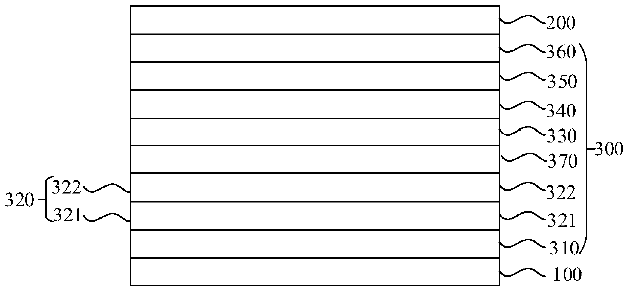
[0265] The anode was prepared by the following process: the thickness was The ITO substrate (manufactured by Corning) was cut into a size of 40mm×40mm×0.7mm, and it was prepared into an experimental substrate with cathode, anode and insulating layer patterns by photolithography process, using ultraviolet ozone and O 2 :N 2 Plasma surface treatment was performed to increase the work function of the anode (experimental substrate) and to remove scum.

[0266] HAT-CN was vacuum evaporated on the experimental substrate (anode) to form a thickness of The hole injection layer (HIL), and compound 1 is vapor-deposited on the hole injection layer to form a thickness of The first hole transport layer (HTL-1).

[0267] TCTA is vacuum evaporated on the first hole transport layer to form a thickness of The second hole transport layer (HTL-2).

[0268] On the second hole transport layer, CBP is used as the host while dopi...

Embodiment 2- Embodiment 22

[0272] An organic electroluminescent device was fabricated by the same method as in Example 1, except that compounds shown in Table 16 below were used instead of Compound 1 when forming the first hole transport layer.

Embodiment 23

[0286] Example 23: Green organic electroluminescence device

[0287] The anode was prepared by the following process: the thickness was The ITO substrate (manufactured by Corning) was cut into a size of 40mm×40mm×0.7mm, and it was prepared into an experimental substrate with cathode, anode and insulating layer patterns by photolithography process, using ultraviolet ozone and O 2 :N 2 Plasma surface treatment was performed to increase the work function of the anode (experimental substrate) and to remove scum.

[0288] Vacuum evaporation of F4-TCNQ on the experimental substrate (anode) to form a thickness of The hole injection layer (HIL), and NPB is evaporated on the hole injection layer to form a thickness of The first hole transport layer (HTL-1).

[0289] Compound 15 is vacuum evaporated on the first hole transport layer to form a thickness of The second hole transport layer (HTL-2).

[0290] On the second hole transport layer, CBP: Ir(ppy) 3 Co-evaporated with a ...


PUM


Abstract

The invention belongs to the field of organic materials, and relates to a spiro compound and an application thereof, and an organic electroluminescent device and an electronic device using the spiro compound. The spiro compound has a structure represented by a formula 1 shown in the description: wherein the group A has a structure represented by a formula 2; and Ar2 is selected from a group consisting of structures shown as a formula a', a formula b', a formula c' and a formula d'. The spiro compound is used as a hole transport material and is applied to an OLED (Organic Light Emitting Diode)device, and a good device performance and relatively low voltage can be obtained.

Description

technical field [0001] The application belongs to the technical field of organic materials, and specifically provides a spiro compound and its application as well as an organic electroluminescence device and an electronic device using the same. Background technique [0002] With the rapid development of information display technology, from computer monitors, to mobile phone screens, to new LCD TVs, they are all application fields of display technology. At present, organic electroluminescent material technology is becoming a research hotspot. OLED has many advantages such as thin and rollable, light weight, fast response, easy processing, low working voltage, etc. It has shown great development potential and market competitiveness, and has also attracted the attention of many scientific researchers. From a technical point of view, compared with other display technologies, OLED has slightly lower technical requirements. At the same time, the development cost of OLED is relat...

Claims


Application Information

Patent Timeline
IPC IPC(8): C07C211/61C07C255/58C07D209/88C07D307/91C07D333/76C07F7/08H01L51/50H01L51/54
CPCC07C211/61C07C255/58C07D209/88C07D307/91C07D333/76C07F7/081C07C2603/94C07C2603/18C07B2200/05H10K85/624H10K85/626H10K85/615H10K85/6576H10K85/6574H10K85/6572H10K85/40H10K50/15
Inventor 杨敏南朋
Owner SHAANXI LIGHTE OPTOELECTRONICS MATERIAL CO LTD
Why Eureka
Try Eureka