Power semiconductor device and manufacturing method thereof

A technology of power semiconductors and manufacturing methods, which is applied in the direction of semiconductor devices, semiconductor/solid-state device manufacturing, electrical components, etc., and can solve problems such as high process costs, low integration of semiconductor devices, and poor electrical performance of power semiconductor devices

Active Publication Date: 2020-07-31
SHANGHAI HUAHONG GRACE SEMICON MFG CORP
View PDF5 Cites 5 Cited by
  • Summary
  • Abstract
  • Description
  • Claims
  • Application Information

AI Technical Summary

Problems solved by technology

The shielded gate polysilicon layer (sourcepoly) of the shielded gate trench (SGT, Split gate trench) in the power semiconductor device cannot be directly drawn out, that is, the connection hole (contact) cannot be directly provided on the shielded gate polysilicon layer, because the connection hole The alignment and CD value have very high requirements, so a special mask is required to define the preset area A (such as Figure 1a As shown), this makes the integration of semiconductor devices lower, and a special photomask is required to form the preset area, making the process cost higher
In addition, when the gate polysilicon layer is formed, the problem of inconsistency of the gate polysilicon layer is prone to occur, resulting in poor electrical performance of the formed power semiconductor device

Method used


Image

  • Power semiconductor device and manufacturing method thereof
  • Power semiconductor device and manufacturing method thereof
  • Power semiconductor device and manufacturing method thereof

Examples


Embodiment Construction

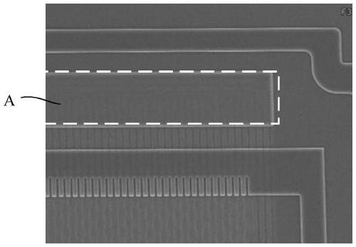
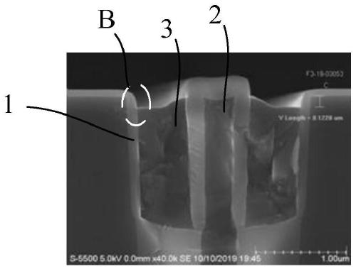
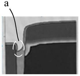
[0043] As mentioned in the background technology, when the gate polysilicon of power semiconductor devices is formed, the problem of inconsistency of the gate polysilicon layer is prone to occur due to the equipment manufacturing process, resulting in poor uniformity of the degree of over-etching of the gate polysilicon layer of the wafer. ,Such as Figure 1b As shown, the thinning of the gate oxide layer tends to occur at the position B of the gate oxide layer 1 on the side of the gate polysilicon layer (gate poly) 3 away from the shield gate polysilicon 2, specifically as Figure 1c As shown, there is a longitudinal defect groove a at the position B of the gate oxide layer 1, and the defect groove a makes the ion implantation process (first p-type ion doping, and then N-type ion doping) when forming the source Doping, the p-type ion-doped region is located below the N-type ion-doped region), N-type ions are implanted into the gate oxide layer 1, which reduces the characteris...


PUM


Abstract

According to the manufacturing method of the power semiconductor device provided by the invention, the side wall is formed on the side wall of the shielding gate polycrystalline silicon layer, and theside wall is positioned above the trench on the outer side of the shield gate polycrystalline silicon layer, so the connecting holes can be directly formed in the shielding gate polycrystalline silicon layer, a mask plate for defining the area where the connecting holes are connected with the gate is omitted, procedures are reduced, the process cost is reduced, and contact between the connectingholes formed in the shielding gate polycrystalline silicon layer subsequently and the gate polycrystalline silicon layer is avoided. The side wall protects the second oxide layer, the subsequent formation of the source electrode is avoided, ions are implanted into the second oxide layer during N-type ion implantation at the upper part, the performance of the second oxide layer is prevented from being reduced, and N-type ions are prevented from scattering downwards through the thinned part of the second oxide layer to enter a P-type ion implantation region during N-type ion implantation, so that the influence of the N-type ions on a channel is avoided, the threshold voltage of the device is improved, and the electrical property of the power semiconductor device is improved.

Description

technical field [0001] The invention relates to the field of semiconductor integrated circuit manufacturing, in particular to a power semiconductor device and a manufacturing method thereof. Background technique [0002] As the integration level of semiconductor devices becomes higher and higher, the pitch of integrated circuits becomes smaller and smaller. The shielded gate polysilicon layer (sourcepoly) of the shielded gate trench (SGT, Split gate trench) in the power semiconductor device cannot be directly drawn out, that is, the connection hole (contact) cannot be directly provided on the shielded gate polysilicon layer, because the connection hole The alignment and CD value have very high requirements, so a special mask is required to define the preset area A (such as Figure 1a As shown), this makes the degree of integration of the semiconductor device lower, and a special photomask is required to form the preset area, which makes the process cost higher. In addition,...

Claims


Application Information

Patent Timeline
Patent Type & Authority Applications(China)
IPC IPC(8): H01L21/336H01L29/78
CPCH01L29/66734H01L29/7813H01L29/66719H01L29/407H01L21/26513H01L21/266H01L21/28132
Inventor 高学
Owner SHANGHAI HUAHONG GRACE SEMICON MFG CORP
Why Eureka
Try Eureka