CMOS-MEMS double-sided integrated chip and integration method thereof

A technology of integrated chips and integrated methods, which is applied in the field of micro-electromechanical systems, can solve the problems of complex sensor structure, difficult completion, and increased chip area, and achieve the effect of reducing the overall volume and solving compatibility problems

Pending Publication Date: 2020-07-31
HEFEI MICRO NANO SENSING TECH CO LTD
View PDF1 Cites 0 Cited by
  • Summary
  • Abstract
  • Description
  • Claims
  • Application Information

AI Technical Summary

Problems solved by technology

However, many sensors with MEMS structures have complex structures, require high-temperature processes, wet etching processes, etc., or produce films with high stress. Such processes are difficult to be compatible with CMOS processes. CMOS and MEMS monolithic integration processes are still a huge challenge. challenge
[0004] At present, CMOS-MEMS monolithic integration in the world usually separates the CMOS and MEMS processes, that is, the CMOS process and the MEMS process are carried out separately. In terms of structure, the CMOS or MEMS process is first completed on the side of the silicon base, leaving another process. The required space is to carry out the next process after the previous process is completed. Although this process achieves the monolithic integration of CMOS and MEMS to a certain extent, the area of ​​the chip will increase a lot
[0005] In order to further solve the problem of increasing the chip area caused by CMOS-MEMS monolithic integration, in recent years, there are patents such as Chinese Patent Publication No. CN108840307A, which propose a method for monolithically integrating CMOS circuits and bulk silicon MEMS, using SOI silicon chips First, make a CMOS circuit on the substrate surface layer of the SOI silicon wafer, and then protect it with an insulating layer to make a MEMS structure on the SOI silicon wafer structure layer
However, this method does not solve the problem of interconnection between CMOS and MEMS circuits, and because the SOI silicon wafer structure layer is usually very thin, it is difficult to complete many MEMS structures that require deep grooves

Method used


Image

  • CMOS-MEMS double-sided integrated chip and integration method thereof
  • CMOS-MEMS double-sided integrated chip and integration method thereof
  • CMOS-MEMS double-sided integrated chip and integration method thereof

Examples


Embodiment 1

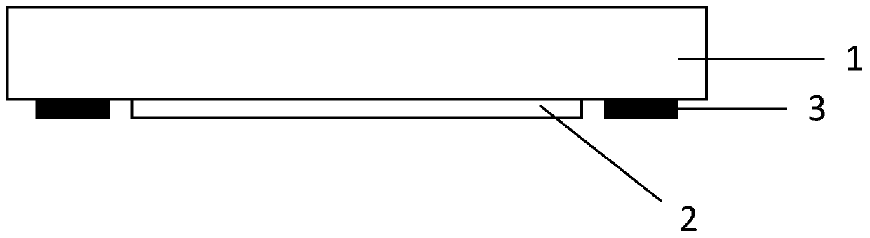
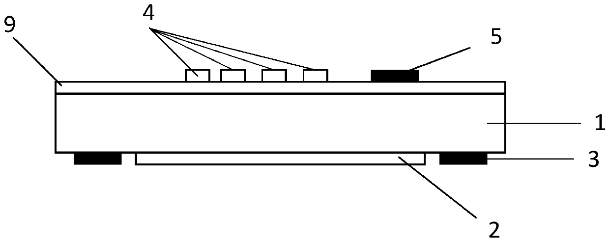
[0044] Such as Figure 5Shown, a kind of CMOS-MEMS double-sided integrated chip comprises substrate 1, CMOS circuit 2, the lead pad 3 of CMOS circuit, MEMS structure 4, the lead pad 5 of MEMS structure, is used for the lead bonding of CMOS circuit The plate 3 leads to the metal via 7 on the surface where the MEMS structure 4 is located. In double-sided boards and multi-layer boards, in order to connect the printed wires between the layers, a common hole is drilled at the intersection of the wires that need to be connected in each layer. , that is, the via hole, and the filling metal in the via hole is the metal via hole. The metal in the metal via hole 7 is one or more of copper, aluminum and gold.

[0045] The substrate 1 in the embodiment of the present invention is a silicon substrate, which is not limited to a silicon substrate in practical applications, and can also be other substrate materials for fabricating MEMS structures and CMOS circuits. The CMOS circuit 2 and th...

Embodiment 2

[0054] Such as Figure 8 As shown, for MEMS, there is also a MEMS structure 4 including a deep cavity 10, so in order to complete the double-sided integration of the MEMS structure 4 including the deep cavity 10 and the CMOS circuit 2, the difference between Embodiment 2 of the present invention and Embodiment 1 is that: The CMOS-MEMS double-sided integrated chip also includes a deep cavity 10, which is opened on the second surface of the substrate 1, and a window 8 is provided on the support layer 9 corresponding to the opening of the deep cavity 10. The depth of the deep cavity 10 is smaller than the thickness of the substrate 1 .

[0055] In practical applications, the window 8 is located in an area other than the MEMS structure 4 on the second surface of the substrate, and the position of the window 8 should not coincide with the position of the MEMS structure 4, so as to avoid accidentally etching off the leads of the MEMS structure 4 to cause circuit failure . Both the...

Embodiment 3

[0058] Corresponding to Embodiment 1 of the present invention, the present invention also provides an integration method of a CMOS-MEMS double-sided integrated chip, the method comprising:

[0059] In order to facilitate the identification of the example diagrams of each process, the steps of the process are identified below, but in practice, the order of the steps is not limited, as long as it meets the process requirements. Such as figure 1 As shown, step a: select a single-throw or double-throw silicon wafer as the substrate 1;

[0060] Such as figure 2 As shown, step b: use the CMOS process to integrate the CMOS circuit 2 and the lead pad 3 of the CMOS circuit on the first surface of the substrate 1; the CMOS process is an existing process flow, including initial cleaning, pre-oxidation, and nitrogen deposition There are dozens of processes such as siliconization, silicon nitride removal, P-well ion implantation, P-well annealing, and oxide layer formation, so I won’t r...


PUM


Abstract

The invention discloses a CMOS-MEMS double-sided integrated chip and an integration method thereof. The CMOS-MEMS double-sided integrated chip comprises a substrate, a CMOS circuit, an MEMS structureand a metal via hole used for leading a lead wire bonding pad of the CMOS circuit to the surface where the MEMS structure is located, wherein the CMOS circuit and the lead wire bonding pad of the CMOScircuit are attached to the first surface of the substrate, the MEMS structure and the lead wire bonding pad of the MEMS structure are attached to the second surface of the substrate, the first surface and the second surface are oppositely distributed, the metal via hole penetrates through the substrate and is communicated with the first surface and the second surface of the substrate, the lead wire bonding pad of the CMOS circuit is located at the position where the metal via hole is located and electrically connected with the metal via hole, and the metal via hole is electrically connectedwith the lead wire bonding pad of the MEMS structure. According to the invention, the CMOS-MEMS double-sided integrated chip has the advantages that CMOS-MEMS double-sided integration and circuit interconnection after double-sided integration are achieved.

Description

technical field [0001] The invention relates to the technical field of micro-electromechanical systems, and more specifically to a CMOS-MEMS double-sided integrated chip and an integration method thereof. Background technique [0002] Micro-Electro-Mechanical Systems (MEMS, Micro-Electro-Mechanical System), also known as micro-electro-mechanical systems, micro-systems, micro-machines, etc., refers to high-tech devices with a size of a few millimeters or even smaller. MEMS is an independent intelligent system whose internal structure is generally on the order of microns or even nanometers. MEMS is developed on the basis of microelectronics technology (semiconductor manufacturing technology), and integrates high-tech electronic machinery produced by technologies such as lithography, corrosion, thin film, LIGA, silicon micromachining, non-silicon micromachining and precision machining. device. MEMS is a revolutionary new technology, widely used in high-tech industries, and a ...

Claims


Application Information

Patent Timeline
Patent Type & Authority Applications(China)
IPC IPC(8): H01L21/48H01L23/538
CPCH01L21/486H01L23/5384
Inventor 陈栋梁谢东成荣钱许磊
Owner HEFEI MICRO NANO SENSING TECH CO LTD
Why Eureka
Try Eureka