Bismuth ferrite film material, method for integrally preparing bismuth ferrite film on silicon substrate at low temperature and application

A bismuth ferrite, silicon-based technology, applied in metal material coating process, ion implantation plating, coating and other directions, can solve the problem of unstable chemical valence and element stoichiometric ratio, and difficulty in obtaining hysteresis of bismuth ferrite film. Line, aggravate leakage, interface diffusion and other problems, to achieve the effects of low cost, reduced volatilization, and easy device integration

Active Publication Date: 2020-08-11
欧阳俊
View PDF11 Cites 2 Cited by
  • Summary
  • Abstract
  • Description
  • Claims
  • Application Information

AI Technical Summary

Problems solved by technology

High heat treatment temperature will not only aggravate leakage, interfacial diffusion and other problems, but also due to the volatile Bi 2 o 3 The loss of defects leads to problems such as defect diffusion, chemical valence and element stoichiometric ratio instability, and high temperature also makes the compatibility of bismuth ferrite film with CMOS-Si technology and large-scale integrated circuits face great challenges.
These problems make it difficult for the bismuth ferrite film to obtain an ideal hysteresis loop and is easy to be broken down, making it difficult to be in line with the application technology. In severe cases, it will lead to device failure

Method used


Image

  • Bismuth ferrite film material, method for integrally preparing bismuth ferrite film on silicon substrate at low temperature and application
  • Bismuth ferrite film material, method for integrally preparing bismuth ferrite film on silicon substrate at low temperature and application
  • Bismuth ferrite film material, method for integrally preparing bismuth ferrite film on silicon substrate at low temperature and application

Examples


Embodiment 1

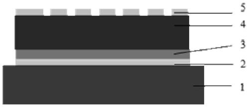
[0049] (a) Treatment of the substrate

[0050] Semiconductor Si / SiO 2 As the substrate, put it into the sample tray, and then put the sample tray into the sample tray rack of the vacuum coating chamber;

[0051] Vacuuming: close the vacuum chamber, evacuate, and make the air pressure in the chamber to ~10 -4 Pa;

[0052] Heating: Introduce Ar into the chamber, the air pressure is 2.3Pa, and then heat the substrate until the temperature rises to 350°C, and then keep the temperature stable.

[0053] (b) Preparation of the bottom electrode

[0054] The bottom electrode was deposited by radio frequency magnetron sputtering with titanium and platinum as sputtering targets. The sputtering gas pressure is adjusted to 0.3Pa, the sputtering power is 55W, and the substrate is sequentially deposited with a total thickness of 150nm.

[0055] (c) Preparation of buffer layer

[0056] The buffer layer was deposited by radio frequency magnetron sputtering with lanthanum nickel oxide cer...

Embodiment 2

[0066] The difference between this embodiment and embodiment 1 is that in step (a), the heating temperature is 400°C.

Embodiment 3

[0068] The difference between this embodiment and embodiment 1 is that in step (d), the thickness of the bismuth ferrite is 60nm.


PUM

PropertyMeasurementUnit
thicknessaaaaaaaaaa
thicknessaaaaaaaaaa
remanent polarizationaaaaaaaaaa

Abstract

The invention discloses a bismuth ferrite film material, a method for integrally preparing a bismuth ferrite film on a silicon substrate at a low temperature and application. The method comprises: under the condition of 300-400 DEG C, a bottom electrode, a buffer layer and a bismuth ferrite film being sequentially subjected to magnetron sputtering on the surface of a base body from bottom to top,reducing the temperature to the room temperature, a top electrode being subjected to magnetron sputtering on the surface of the bismuth ferrite film, and the buffer layer being made of conductive oxide which can be matched with bismuth ferrite lattices and is of a perovskite structure. The temperature for preparing the bismuth ferrite film material can be reduced to 450 DEG C or below, and the bismuth ferrite film material has high polarization strength.

Description

technical field [0001] The invention relates to the development of electronic materials and the preparation technology of thin film materials, in particular to a bismuth ferrite film material, a method for integrated preparation of bismuth ferrite film on a silicon substrate at low temperature and its application. Background technique [0002] The information disclosed in this background section is only intended to increase the understanding of the general background of the present invention, and is not necessarily taken as an acknowledgment or any form of suggestion that the information constitutes the prior art already known to those skilled in the art. [0003] In recent years, ferroelectric materials, especially ferroelectric films, have a wide range of applications in high-capacity memories, high-density capacitors, and micro-electromechanical systems due to their excellent ferroelectric, piezoelectric, dielectric, photoelectric, and pyroelectric properties. The applica...

Claims


Application Information

Patent Timeline
Patent Type & Authority Applications(China)
IPC IPC(8): H01L41/316H01L41/187C23C14/08C23C14/16C23C14/35
CPCC23C14/0036C23C14/35C23C14/165C23C14/08H10N30/8561H10N30/076C23C14/024C23C14/5853C23C14/541C23C14/02C23C14/042C23C14/16C23C14/3414C23C14/352
Inventor 欧阳俊牛淼淼朱汉飞
Owner 欧阳俊
Why Eureka
Try Eureka