Self-alignment preparation method of drain terminal negative overlapping region of tunneling transistor

A technology of tunneling transistors and overlapping regions, which is applied in semiconductor/solid-state device manufacturing, semiconductor devices, electrical components, etc., and can solve problems affecting device contact, unfavorable device consistency, and impurity segregation Pole effect, good consistency, and the effect of optimizing device fluctuation characteristics

Inactive Publication Date: 2020-08-21
PEKING UNIV
View PDF4 Cites 1 Cited by
  • Summary
  • Abstract
  • Description
  • Claims
  • Application Information

AI Technical Summary

Problems solved by technology

However, this method will make the doping of the device heavily dependent on the lithography accuracy, and will introduce additional fluctuation sources, which is not conducive to the consistency of the device and affects the large-scale integration application of TFET devices.
And the use of this method is not conducive to the metal silicide treatment of the device, which affects the contact of the device, and is not conducive to the use of technologies such as impurity segregation

Method used


Image

  • Self-alignment preparation method of drain terminal negative overlapping region of tunneling transistor
  • Self-alignment preparation method of drain terminal negative overlapping region of tunneling transistor
  • Self-alignment preparation method of drain terminal negative overlapping region of tunneling transistor

Examples


Embodiment Construction

[0041] The present invention will be further described below by example. It should be noted that the purpose of the disclosed embodiments is to help further understand the present invention, but those skilled in the art can understand that various replacements and modifications are possible without departing from the spirit and scope of the present invention and the appended claims of. Therefore, the present invention should not be limited to the content disclosed in the embodiments, and the protection scope of the present invention is subject to the scope defined in the claims.

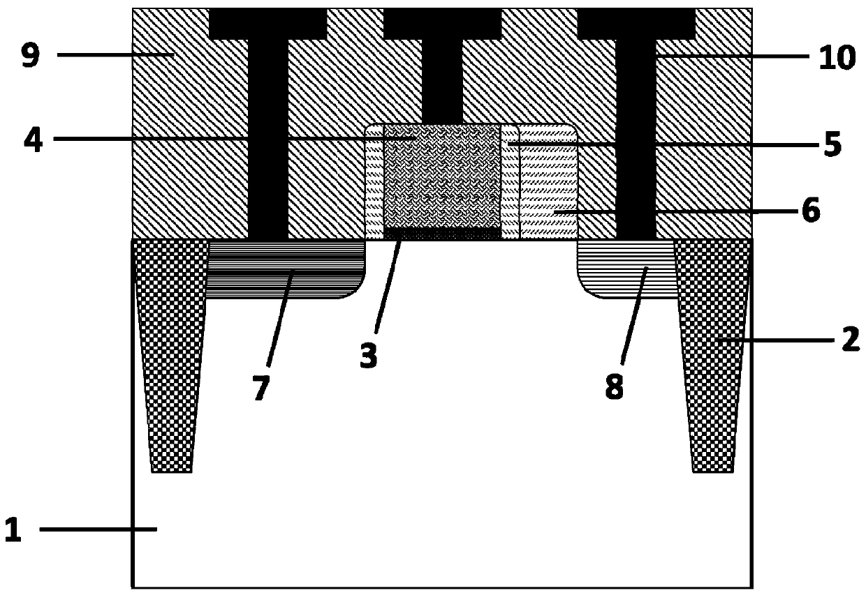
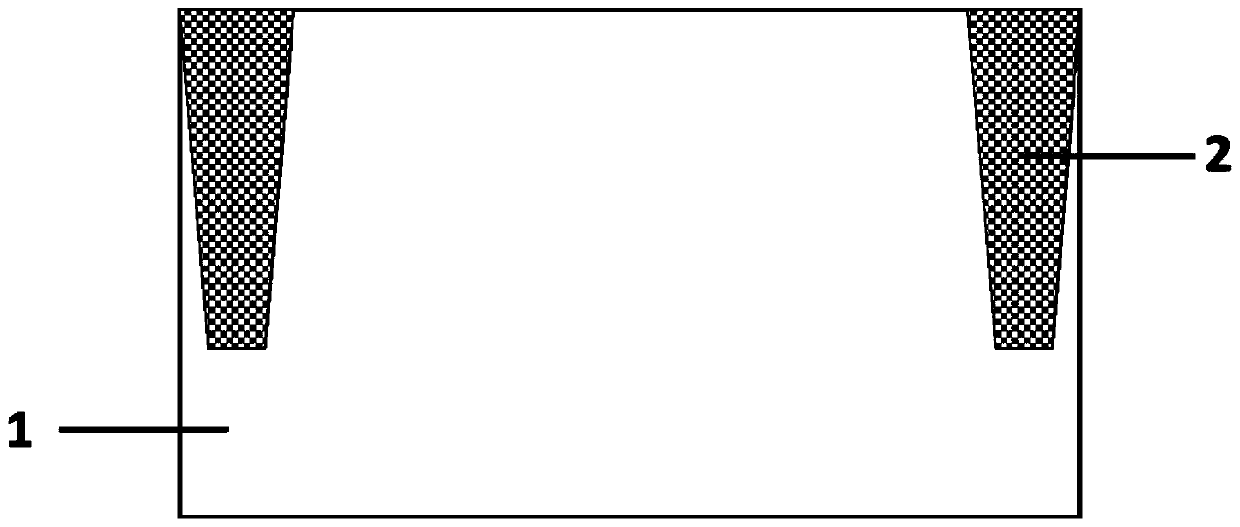
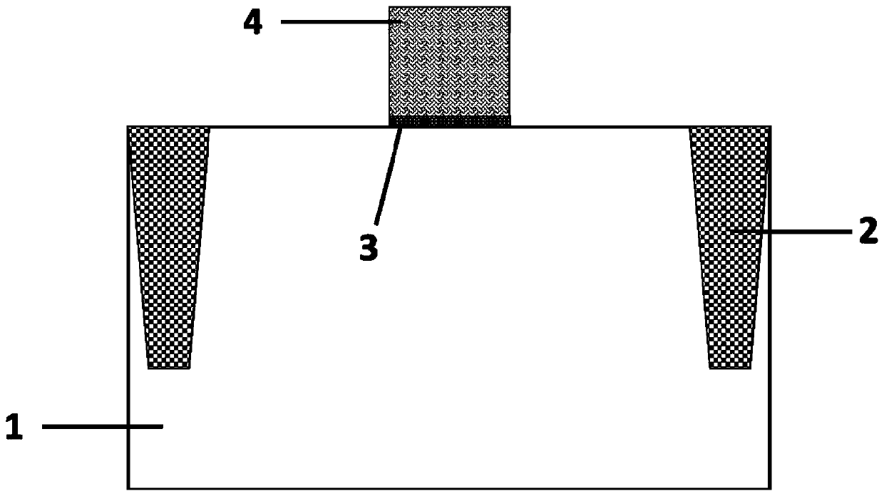
[0042] A specific example of the preparation method of the present invention includes Figure 1 to Figure 7 Process steps shown:

[0043] 1. Initially thermally oxidize a layer of silicon dioxide with a thickness of about 10 nm on a bulk silicon substrate 1 with a lightly doped substrate doping concentration and a crystal orientation of , and deposit a layer of silicon nitride with a thickness of a...


PUM

PropertyMeasurementUnit
thicknessaaaaaaaaaa
thicknessaaaaaaaaaa
thicknessaaaaaaaaaa

Abstract

The invention discloses a self-alignment preparation method for a self-alignment gate-drain negative overlapping region of a tunneling field effect transistor, and belongs to the field of field effecttransistor logic devices and circuits in a CMOS ultra-large integrated circuit (ULSI). According to the method, asymmetric side wall structures are designed on the two sides of a tunneling transistorgate, the side, close to a source end, of the gate is a thin side wall, and the side, close to a drain end, of the gate is a thick side wall. According to the invention, by reasonably utilizing the thin side wall and the thick side wall in the standard CMOS process, the thin side wall at the source end is used as a hard mask for transistor source region injection, and the thick side wall at the drain end is used as a hard mask for transistor drain region injection, so that special materials and special processes are not introduced, the bipolar effect of a tunneling field effect transistor (TFET) is inhibited, the fluctuation characteristic of the device is optimized, it can be guaranteed that the TFET can be mixed and integrated with a standard CMOS device, and complex and diversified circuit functions are achieved.

Description

technical field [0001] The invention belongs to the field of field effect transistor logic devices and circuits in a CMOS ultra large integrated circuit (ULSI), and in particular relates to the design and preparation of a drain terminal negative overlap region of a tunneling transistor. Background technique [0002] With the continuous development of integrated circuits, the feature size of devices continues to decrease, and the power consumption density of chips continues to increase. Circuit power consumption has gradually become an important factor limiting the scaling down of integrated circuits. In order to reduce the power consumption of the circuit, a better way is to reduce the power supply voltage. However, the subthreshold slope of the MOSFET is limited by the thermoelectric potential, which cannot be lower than 60mV / dec at room temperature. In the case of maintaining a certain driving capability, further reducing the power supply voltage will lead to an exponentia...

Claims


Application Information

Patent Timeline
Patent Type & Authority Applications(China)
IPC IPC(8): H01L29/78H01L29/417H01L21/336H01L29/06
CPCH01L29/78H01L29/41725H01L29/41758H01L29/41766H01L29/66477H01L29/0684H01L29/0603H01L29/7391H01L29/66356H01L21/28052H01L21/76897H01L21/823443H01L29/4933H01L29/66507H01L29/6659
Inventor 黄芊芊李一庆杨勐譞王志轩叶乐蔡一茂黄如
Owner PEKING UNIV
Why Eureka
Try Eureka