Integrated Optical Autocorrelator Based on Transverse Double Frequency Effect of Two-dimensional Materials

An integrated optics and autocorrelator technology, applied in optics, optical components, nonlinear optics, etc., can solve the problems of large insertion loss of devices, high requirements for delay adjustment accuracy, and poor time resolution, and achieve a high degree of integration. High, the effect of eliminating the delay

Active Publication Date: 2021-04-13
ZHEJIANG UNIV
View PDF8 Cites 0 Cited by
  • Summary
  • Abstract
  • Description
  • Claims
  • Application Information

AI Technical Summary

Problems solved by technology

However, in the above-mentioned on-chip ultrashort pulse measurement method, the integration degree of the former is not high, and more devices (such as polarization controllers, optical fiber beam splitters, optical attenuators, delayers, etc.) need to be used outside the substrate, By adjusting the time delay to control the pulse light on both sides of the waveguide to meet and excite the third harmonic in the waveguide, the accuracy of the time delay adjustment is relatively high. At the same time, the production accuracy of the photonic crystal waveguide is relatively high, and the insertion loss of the device is relatively large. The linear conversion efficiency is not high; the latter has poor time resolution and complicated manufacturing process

Method used


Image

  • Integrated Optical Autocorrelator Based on Transverse Double Frequency Effect of Two-dimensional Materials
  • Integrated Optical Autocorrelator Based on Transverse Double Frequency Effect of Two-dimensional Materials
  • Integrated Optical Autocorrelator Based on Transverse Double Frequency Effect of Two-dimensional Materials

Examples


Embodiment approach

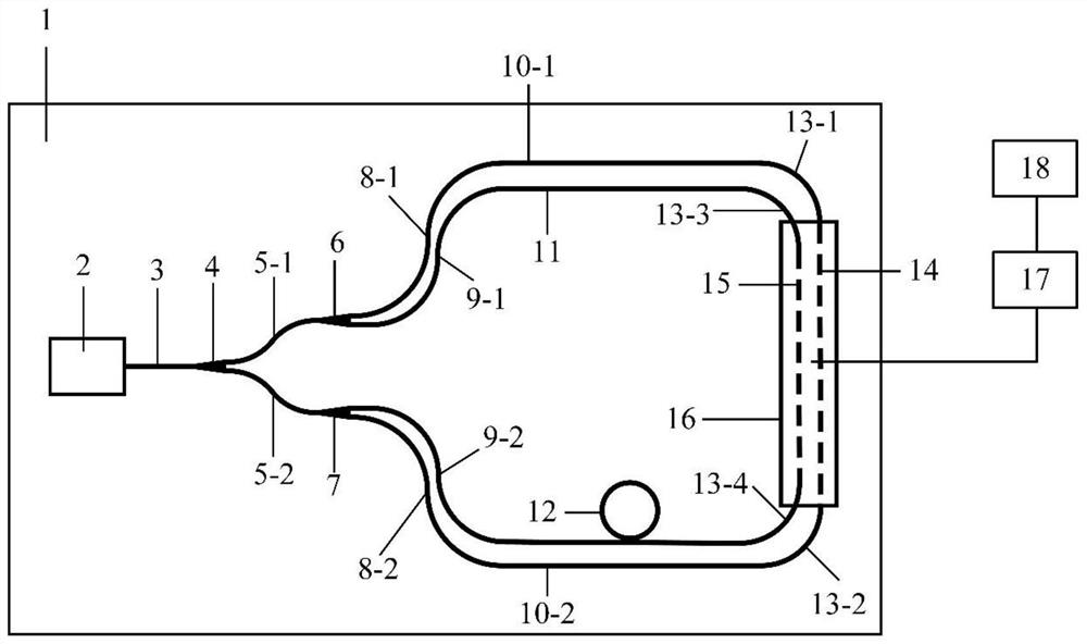
[0022] see figure 1, as the first embodiment of the present invention, the integrated optical autocorrelator based on the transverse double frequency effect of two-dimensional materials includes a substrate 1, an on-chip coupling system, a two-dimensional material film 16, a convex lens 17 and an imaging camera 18; on-chip coupling The system includes a grating coupler 2, a first beam splitter 4, a second beam splitter 6, a third beam splitter 7, a first S-shaped waveguide 8-1, a second S-shaped waveguide 8-2, and a third S-shaped waveguide Waveguide 9-1, fourth S-shaped waveguide 9-2, first arcuate waveguide 13-1, second arcuate waveguide 13-2, third arcuate waveguide 13-3, fourth arcuate waveguide 13-4. The first straight waveguide 14, the second straight waveguide 15 and the delayer 12, wherein the first beam splitter 4, the second beam splitter 6 and the third beam splitter 7 are 50:50 1× 2 beam splitters. The output end of the grating coupler 2 is connected with the inp...


PUM

PropertyMeasurementUnit
widthaaaaaaaaaa
thicknessaaaaaaaaaa

Abstract

The invention discloses an integrated optical autocorrelator based on the transverse doubling frequency effect of two-dimensional materials, comprising a substrate, an on-chip coupling system integrated on the substrate, a two-dimensional material film, a convex lens and an imaging camera; the on-chip coupling system includes a grating Coupler, three 1×2 beam splitters with a beam splitting ratio of 50:50, the first S-shaped waveguide, the second S-shaped waveguide, the third S-shaped waveguide, the fourth S-shaped waveguide, and the first arc-shaped waveguide , the second arc-shaped waveguide, the third arc-shaped waveguide, the fourth arc-shaped waveguide, the first straight waveguide and the second straight waveguide; the two-dimensional material film is a single-layer film with second-order nonlinear effect, and the two-dimensional The material film completely covers the first straight waveguide and the second straight waveguide, and the frequency-doubled light excited by the two-dimensional material film enters the imaging camera through the convex lens for imaging. The invention has high time resolution and greatly improves the integration degree of the on-chip coupling system, and can save the delay device commonly used in the prior art, and has low cost and wide application range.

Description

technical field [0001] The invention relates to a two-dimensional material and a micro-nano photon integrated device, in particular to an integrated optical autocorrelator, which belongs to the field of ultrashort pulse measurement. Background technique [0002] Ultrashort pulsed light plays an important role in ultrafast spectroscopy, strong field physics, optical communication, biomedicine and other fields. In recent years, optical autocorrelation measurement methods for ultrashort pulse measurements have been widely studied and applied. With the development of micro-nano photonic integration technology, on-chip ultrashort pulse measurement technology is conducive to providing a flexible integration platform to realize an optical chip integrating pulse generation, optical processing and measurement modules. There are two types of existing integrated optical autocorrelators: one is based on the third harmonic effect of the lateral emission of the photonic crystal silicon w...

Claims


Application Information

Patent Timeline
Patent Type & Authority Patents(China)
IPC IPC(8): G02B6/12G01J11/00G02F1/37G02B6/26
CPCG01J11/00G02B6/12004G02B6/26G02F1/37
Inventor 郭欣张建彬童利民鲍庆洋吴昊李维嘉石章兴
Owner ZHEJIANG UNIV
Why Eureka
Try Eureka