PCB solder mask production process

A production process and solder mask technology, applied in the secondary processing of printed circuits, electrical components, metallurgical bonding, etc., can solve the problems of low production efficiency, large water and electricity consumption, and high production costs, saving water, electricity, labor, and energy. Consumption and labor saving effect

Inactive Publication Date: 2020-09-08
江西兆信精密电子有限公司
View PDF5 Cites 5 Cited by
  • Summary
  • Abstract
  • Description
  • Claims
  • Application Information

AI Technical Summary

Problems solved by technology

[0004] The traditional PCB production process produces many pollutants, among which the production processes such as electroplating, wiring, and solder mask produce the most pollutants; and the traditional PCB production process also consumes a lot of water and electricity
For example, the traditional solder resist process needs to use special PCB inks for printing, pre-baking, alignment, exposure, development, post-baking and other processes to make pad windows. This process consumes a lot of hydropower and energy and has low production efficiency. Moreover, a large amount of organic waste water and waste gas are produced, and the production cost is also high.

Method used


Image

  • PCB solder mask production process
  • PCB solder mask production process
  • PCB solder mask production process

Examples


Embodiment

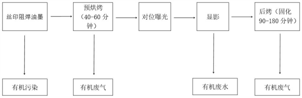
[0027] A PCB welding mask production process, comprising the following steps:

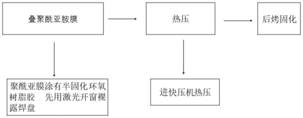
[0028] S1. Prepare raw materials, prepare a polyimide film coated with semi-cured epoxy resin glue or semi-solid acrylic on one side, prepare a PCB substrate that needs to be soldered, and combine the prepared polyimide film with the PCB Segmentation of the substrate into the size to be produced;

[0029] S2, the exposed pad, the polyimide film coated with semi-cured epoxy resin glue or coated with semi-cured acrylic in step S1 is windowed by laser to form a windowed pad on the surface, and multiple groups of polyimide The window pad size parameters of the amine film remain the same;

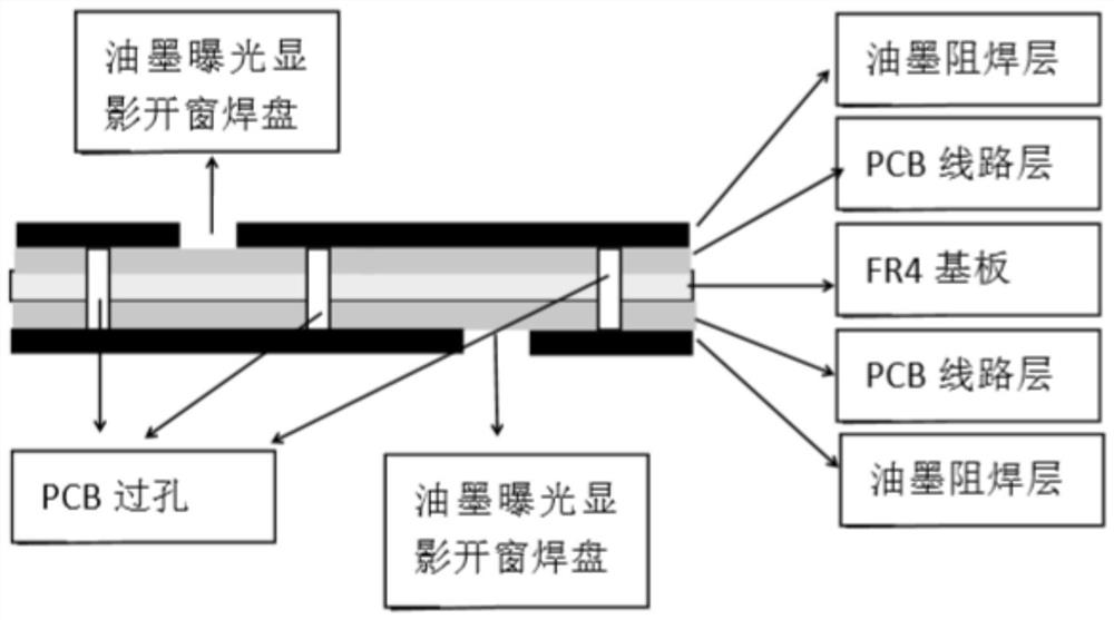
[0030] S3, stacking the films, stacking multiple groups of polyimide films with consistent window pads in step S2, and ensuring that the multiple groups of polyimide films are aligned consistently to form a laminated structure A;

[0031] S4, fixing the stacked film, and stacking the stacked structure A formed by s...


PUM

PropertyMeasurementUnit
thicknessaaaaaaaaaa

Abstract

The invention discloses a PCB solder mask production process. The PCB solder mask production process comprises the following steps of: raw material preparation, bonding pad exposing, film stacking, stacked film fixing, high-temperature hot press molding, baking and curing. Compared with the traditional PCB production process, the PCB solder mask production process provided by the invention has theadvantages that zero emission is realized through the solder mask process, water and electricity are saved, and the production cycle of the process can be greatly shortened; the PCB can be enabled tohave a considerable bending property; the production process comprises the following steps of: coating one sides of polyimide films (PI) with a semi-cured epoxy resin adhesive (or semi-solid acrylicacid), cutting windowing positions of PCB bonding pads on the polyimide films (PI) by processes like laser or die punching, then stacking and fixing the windowed polyimide films (PI) on a PCB body ina stacking mode, and performing pressing and forming in a high-temperature fast pressing mode, thus finally obtaining a solder mask superior to printing ink. The process saves water, electricity and labor, improves the production efficiency, and is environment-friendly and pollution free.

Description

technical field [0001] The invention belongs to the technical field of PCB solder mask production, and more specifically relates to a PCB solder mask production process. Background technique [0002] PCB is a printed circuit board, referred to as a printed board, and is one of the important components of the electronics industry. Almost every kind of electronic equipment, ranging from electronic watches and calculators to computers, communication electronic equipment, and military weapon systems, as long as there are electronic components such as integrated circuits, in order to make the electrical interconnection between various components, printed circuit boards must be used. plate. The printed circuit board is composed of an insulating base plate, connecting wires and pads for assembling and welding electronic components, and has the dual functions of a conductive line and an insulating base plate. It can replace complex wiring and realize the electrical connection betw...

Claims


Application Information

Patent Timeline
Patent Type & Authority Applications(China)
IPC IPC(8): H05K3/28H05K3/32
CPCH05K3/281H05K3/328H05K2203/04
Inventor 郭兆华
Owner 江西兆信精密电子有限公司
Why Eureka
Try Eureka