Supercharge Your Innovation With Domain-Expert AI Agents!

Method for calculating and regulating perovskite material defects based on first principle

A perovskite material and a first-of-its-kind technology, which is applied in the field of perovskite material defect calculation based on first-principle calculations, can solve problems such as uneven doping in the crystallized part of the region, affecting photoelectric properties, etc., so that the process is easy to control, Reduce costly effects

Pending Publication Date: 2020-09-11
XIDIAN UNIV
View PDF4 Cites 2 Cited by
  • Summary
  • Abstract
  • Description
  • Claims
  • Application Information

AI Technical Summary

Problems solved by technology

[0004] Zheng Zhiping, Chen Hualin and others reported a method to improve the resistivity of cesium bromide and lead. By doping monovalent cation Ag, the resistivity and carrier migration life of the material were improved, making it better used in high-energy rays. In terms of detectors, but the uneven doping of the crystal part may affect the photoelectric properties

Method used


Image

  • Method for calculating and regulating perovskite material defects based on first principle
  • Method for calculating and regulating perovskite material defects based on first principle
  • Method for calculating and regulating perovskite material defects based on first principle

Examples


Embodiment

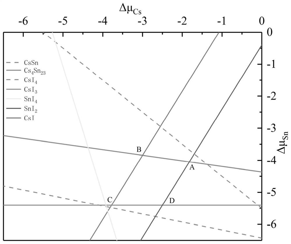
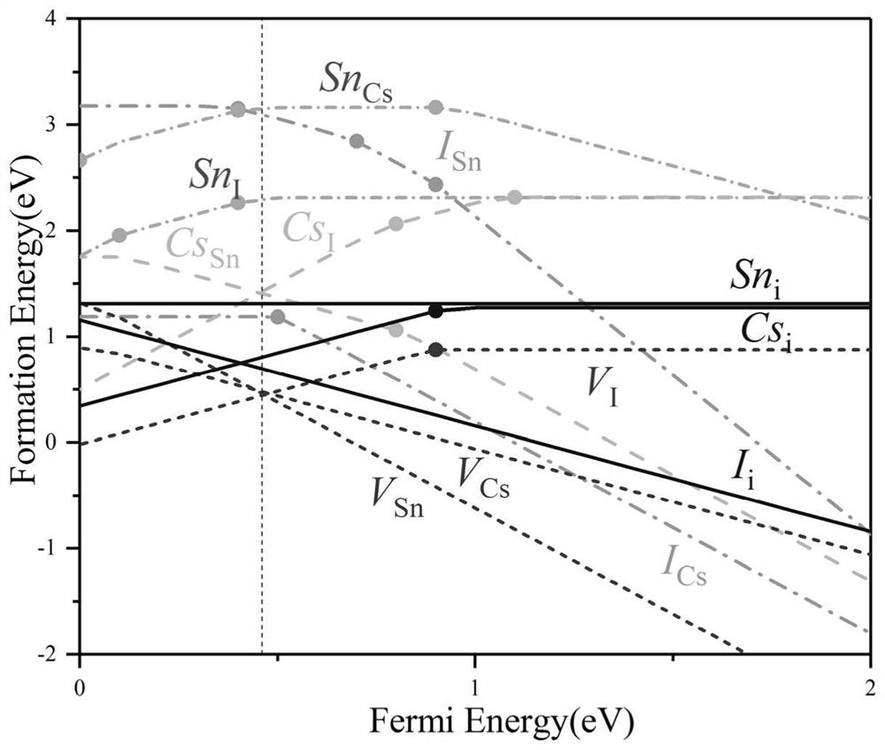
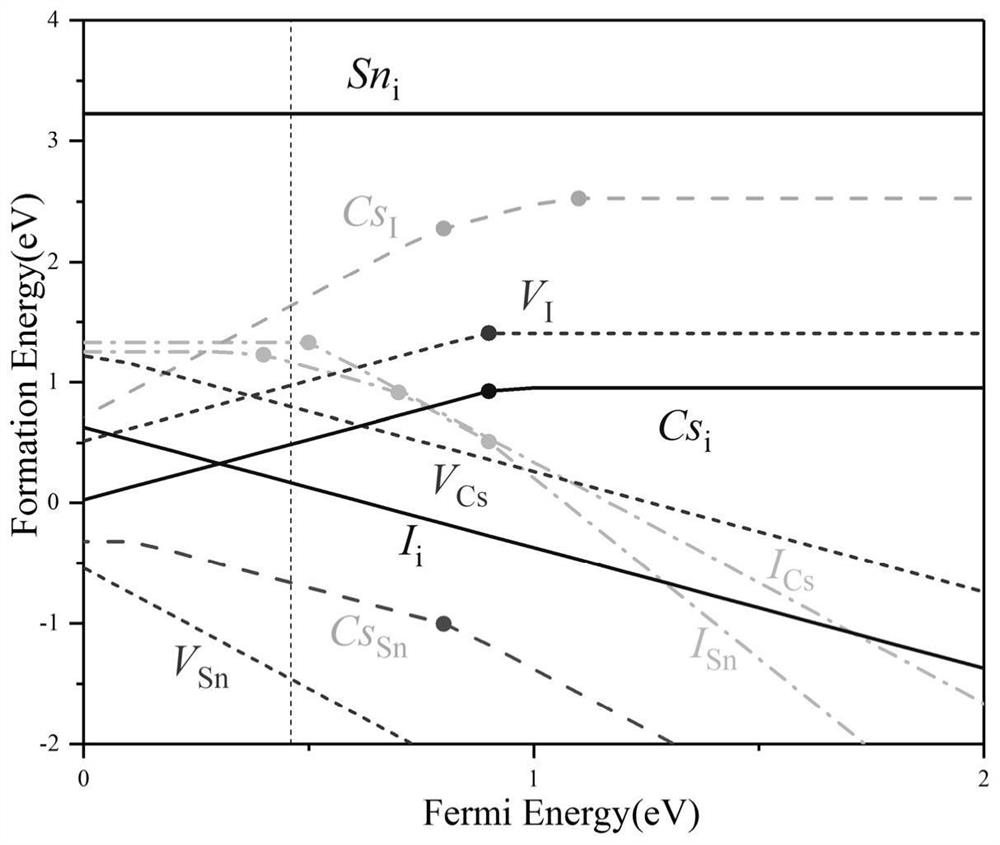
[0043] A method for controlling defects in perovskite materials based on first-principles calculations, see Figure 1~4 As shown, it specifically includes the following steps:

[0044] Step 1, the chemical formula is ABX 3 Construction of a perovskite crystal system defect model.

[0045] ABX 3 Perovskite crystal defect model using CsSnI 3 The face-centered cubic crystal system, a total of twelve defect models include: V Cs , V Sn , V I 、Cs i , Sn i , I i、Cs Sn , I Cs , I Sn , Sn I , Sn Cs 、Cs I .

[0046] The crystal structure three-dimensional software Materials Studio was used to construct the unit cells of ideal crystals and defective crystals.

[0047] Use VESTA to convert the constructed 3D crystal structure from the .cif file exported in Materials Studio to a .vasp file.

[0048] The defect model adopts the most stable state model.

[0049] The .vasp files described use inverted lattice arrows.

[0050] Step 2, simulate the free energy and ABX of the ...


PUM


Abstract

The invention discloses a method for calculating and regulating perovskite material defects based on a first principle, and belongs to the technical field of new materials. The method comprises the following steps: S1, constructing a defect crystal model of perovskite crystal system supercells by utilizing MS software, and converting a structure data file type into a .Vasp file format by virtue ofVESTA software; S2, performing first principle calculation simulation on the intermediate product crystal model and the defect crystal model; S3, preparing an intermediate product and a final productby linear programming analysis to form constraint conditions, quantifying defect crystal formation energy in the constraint conditions, and quantifying an energy level position in a defect crystal bythe defect crystal formation energy; and S4, changing the variables in the constraint conditions, and analyzing the change of the formation energy and the energy level position of the defect crystalso as to play a role in regulating and controlling the defects of the perovskite material. The invention discloses the formation rule of spontaneous defects and deep and shallow energy levels in the perovskite diffusion material, and required material characteristics can be obtained through regulation and control.

Description

technical field [0001] The invention belongs to the technical field of new materials, and in particular relates to a method for calculating and regulating defects of perovskite materials based on first principles. Background technique [0002] As a new type of material, perovskite is widely used, not only as a light-absorbing layer material for solar cells, but also in light-emitting diodes, semiconductor lasers, and photovoltaic detectors. Devices made of perovskite materials are low in cost, high in efficiency and easy to prepare as a light-absorbing layer material, adjustable in spectrum as a light-emitting diode, and wide in spectrum coverage as a photovoltaic detector. However, for semiconductor materials, the generation of intrinsic defects is inevitable, and a small amount of defects often has a huge impact on the performance of semiconductor devices. [0003] The current research on perovskite materials in optoelectronics and optoelectronics is that it is mainly an ...

Claims


Application Information

Patent Timeline
IPC IPC(8): G16C60/00G16C10/00
CPCG16C60/00G16C10/00Y02E10/549
Inventor 苏杰林珍华常晶晶张钧瑜郝跃
Owner XIDIAN UNIV
Features
  • R&D
  • Intellectual Property
  • Life Sciences
  • Materials
  • Tech Scout
  • Unparalleled Data Quality
  • Higher Quality Content
  • 60% Fewer Hallucinations
Learn More