Method for detecting photoelectric property of microcell of a photoelectric material

A technology of optoelectronic materials and optoelectronic properties, applied in the field of photoelectrochemistry

Pending Publication Date: 2020-09-15
SHANGHAI UNIV
View PDF7 Cites 6 Cited by
  • Summary
  • Abstract
  • Description
  • Claims
  • Application Information

AI Technical Summary

Problems solved by technology

[0005] In view of the above-mentioned defects of the prior art, the technical problem to be solved by the present invention is how to measure the photoelectric performance difference corresponding to the different surface micro-topography of the material micro-region, and how to detect the photoelectric performance distribution of grain boundaries and different grain orientations.

Method used


Image

  • Method for detecting photoelectric property of microcell of a photoelectric material
  • Method for detecting photoelectric property of microcell of a photoelectric material
  • Method for detecting photoelectric property of microcell of a photoelectric material

Examples


Embodiment 1

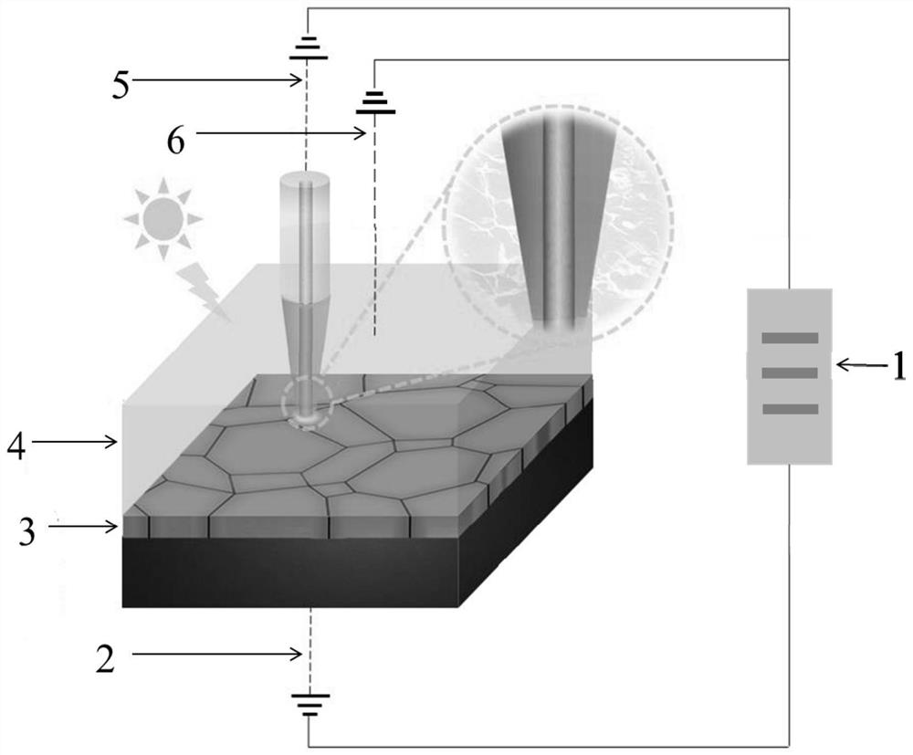
[0034] Acetonitrile solution and 0.1 mol / L tetrabutylammonium hexafluorophosphate are configured as supporting electrolyte, 0.05 mol / L ferrocene is redox agent, in the photoelectrochemical reaction solution containing oxidation or reducing agent as mentioned above , the polysilicon film material to be measured is fixed on the bottom of the photoelectrochemical reaction zone 4, the microelectrode probe 5 (platinum electrode, 3 μm in diameter) is used as the working electrode, and silver / silver nitrate is the reference electrode 6. The polysilicon to be measured The membrane material is the counter electrode 2, which constitutes a photoelectrochemical test cell. The microelectrode probe 5 is connected with the scanning electrochemical microscope control system 1 to form a precise control scanning mobile platform, and the movement is precisely controlled by the scanning electrochemical microscope so that the microelectrode probe 5 is close to the surface of the photoelectric film ...

Embodiment 2

[0036]Acetonitrile and 0.1 mol / liter tetrabutylammonium hexafluorophosphate are configured as supporting electrolyte, 0.05 mol / liter ferrocene is used as redox agent, silver / silver nitrate electrode is selected as reference electrode 6, and platinum electrode is used as counter electrode. The electrode 2, the platinum wire is the working electrode 7, and the optical fiber with a diameter of 3 microns is the optical fiber microprobe 8. The polysilicon film material to be measured is fixed on the bottom of the photoelectrochemical reaction zone 4, and the three-electrode system in the scanning electrochemical microscope system is sequentially connected with the silver / silver nitrate reference electrode 6, the platinum counter electrode 2, and the polysilicon film material working electrode 7 connected. At the same time, the optical fiber microprobe 8 is connected with the scanning electrochemical microscope control system 1 to form a precisely controlled scanning mobile platform...


PUM

PropertyMeasurementUnit
diameteraaaaaaaaaa

Abstract

The invention discloses a method for detecting the photoelectric property of a microcell of a photoelectric material, and relates to the technical field of photoelectrochemistry. On the basis of a scanning electrochemical microscope device, an optical fiber microprobe and a microelectrode probe are adopted, and a sample microcell (including crystal grains, crystal boundaries and the like) is accurately scanned in a photoelectrochemical cell, so that the photoelectrochemical performance of the material microcell is obtained. According to the method for detecting the photoelectric property of microcell of a photoelectric material , the photoelectric property differences corresponding to different surface microstructures of the material microcell can be measured; and the photoelectric property distribution of grain boundaries and different grain orientations is detected, so that the limitation that only the overall macroscopic photoelectric property of the material can be measured in thetraditional method is eliminated. The method has important guiding significance for photoelectric conversion mechanism research and process performance improvement.

Description

technical field [0001] The invention relates to the field of photoelectrochemical technology, in particular to a method for detecting photoelectric properties of photoelectric material micro-regions. Background technique [0002] With the depletion of fossil fuel energy, solar energy, which is an inexhaustible source of energy for nature, has attracted more and more researchers' attention, followed by the rise of photovoltaic energy technology research boom . Theoretical studies have shown that the relationship between the microdomain / grain boundary morphology and optoelectronic performance of optoelectronic materials is very important. [0003] Traditional methods for studying photoelectrochemical properties mainly include spectroscopy and electrochemical methods. The former type of methods mainly include transient absorption spectrometer, ultraviolet-visible spectrophotometer and fluorescence photometer. The latter method mainly uses various electrochemical measurement ...

Claims


Application Information

Patent Timeline
Patent Type & Authority Applications(China)
IPC IPC(8): G01Q30/02G01Q30/20G01N27/26G01N27/30
CPCG01Q30/02G01Q30/20G01N27/26G01N27/30
Inventor 邹星礼唐蔚庞忠亚李想汪淑娟卢明辉许茜鲁雄刚
Owner SHANGHAI UNIV
Why Eureka
Try Eureka