Manufacturing method of nanofiber probe tip for measuring surface topography of sample

A surface topography measurement and nanofiber technology, which is applied in measuring devices, scanning probe technology, scanning probe microscopy, etc., can solve problems such as low utilization rate, cumbersome process, and strict requirements for precision in nanostructure scanning. Achieve the effect of high utilization rate and strong robustness

Active Publication Date: 2020-09-22
INST OF MECHANICS - CHINESE ACAD OF SCI
View PDF7 Cites 3 Cited by
  • Summary
  • Abstract
  • Description
  • Claims
  • Application Information

AI Technical Summary

Problems solved by technology

The performance of the atomic force microscope is closely related to the probe used. Due to the limitation of the probe preparation process, the minimum size of the probe tip on the market is about 10 nanometers, which is difficult to meet the stringent requirements for the accuracy of nanostructure scanning. The current general practice It is to bond nanostructures (such as carbon nanotubes) to the tip of the probe (Chinese patent application number: CN107436366A)
At present, there are three mainstream preparation methods. The first method is to modify the tip of an ordinary probe, bond a catalyst, and then put the nanotube into it for reaction, so that the carbon nanotube grows at the tip (CN1232813C). It is cumbersome, has high requirements for instruments, and is only suitable for bonding carbon nanotubes at the tip of the needle; the second method is to suspend the nanostructure to be adsorbed on the surface of the liquid, and then let the tip of the needle touch the water surface, so that the nanostructure suspended on the water surface The structure is adsorbed at the tip of the needle (LeeJH, KangWS, ChoiBS, etc., Ultramicroscopy, (2008) 108: 1163-1167.). This method has strict requirements on the density of the liquid and the density of the nanostructure on the water surface. Therefore, the density of the material during the preparation process The consumption is large, the utilization rate is low, and the bonding position and direction of the nanostructure cannot be controlled; the third method uses the polarity of the fiber to adsorb the probe to the tip of the probe through the tip electric field (TangJ, YangG, ZhangQ, etc. , Nanoletters (2005) 5: 11-14; StevensRM, Materialstoday, (2009) 12: 42-45), but this method is only applicable to polar materials, such as carbon nanotubes, so the scope of application is limited

Method used


Image

  • Manufacturing method of nanofiber probe tip for measuring surface topography of sample
  • Manufacturing method of nanofiber probe tip for measuring surface topography of sample
  • Manufacturing method of nanofiber probe tip for measuring surface topography of sample

Examples


Embodiment 1

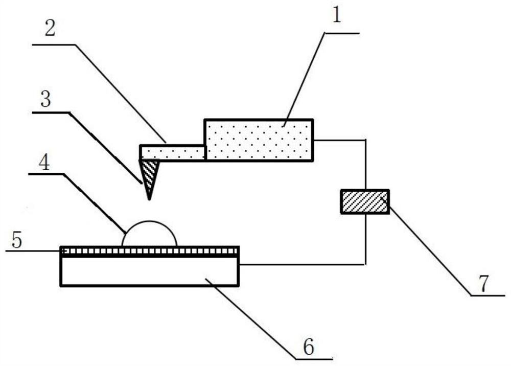
[0042] like figure 1 As shown, a nanofiber probe tip manufacturing equipment for sample surface topography measurement, specifically includes: probe, probe clamping mechanism, substrate support mechanism, power supply,

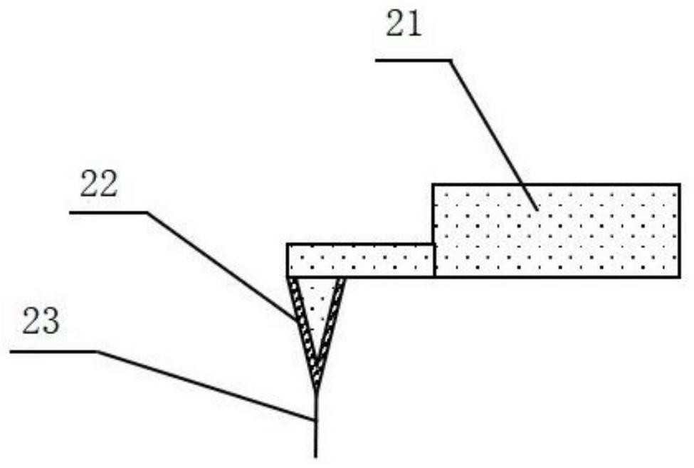
[0043] The probe includes a needle body and a conductive layer, and the conductive layer is coated on the surface of the needle body;

[0044] The probe clamping mechanism includes a probe clamping end and a probe cantilever beam installed at the end, and the probe is vertically suspended and installed on the probe cantilever beam;

[0045] The base support mechanism includes a conductive plate and a dielectric layer, and the dielectric layer is coated on the surface of the conductive plate;

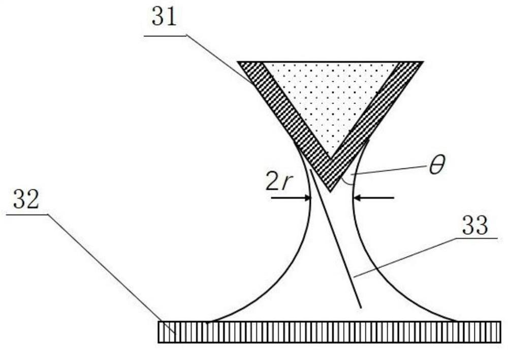
[0046] Connect the probe and conductive plate to both ends of the power supply;

[0047]The suspended liquid drops are formed on the surface of the base support mechanism, the power is turned on, and the probe is controlled by the probe clamping mechanism to slowly app...

Embodiment 2

[0056] like Figure 4 Shown, a kind of nanofiber probe tip manufacturing method for sample surface topography measurement, the method comprises the following steps:

[0057] 1) Prepare the substrate: prepare a conductive flat plate, the roughness Ra of the conductive flat plate should be less than 0.1 micron, the material of the conductive flat plate can be any conductive solid, and the size of the flat plate is not strictly required. It is carried out under a microscope, so the recommended size is 10*10*0.5 mm, and the surface of the flat plate is covered with a non-conductive material as a dielectric layer. The thickness and covering method of the dielectric layer are related to the material selected, usually the thickness ranges from 100 to 60,000 nanometers, it is recommended to use the suspension coating method to attach polydimethylsiloxane PDMS (the mass ratio of PDMS and crosslinking agent is 10:1) to the surface of the conductive plate, the thickness of the suspension...

Embodiment 3

[0067] like Figure 4 Shown, a kind of nanofiber probe tip manufacturing method for sample surface topography measurement, the method comprises the following steps:

[0068] 1) Prepare the substrate: prepare a conductive flat plate, the roughness Ra of the conductive flat plate should be less than 0.1 micron, the material of the conductive flat plate can be any conductive solid, and the size of the flat plate is not strictly required. It is carried out under a microscope, so the recommended size is 10*10*0.5 mm, and the surface of the flat plate is covered with a non-conductive material as a dielectric layer. The thickness and covering method of the dielectric layer are related to the material selected, usually the thickness ranges from 100 to 60000 nanometers, it is recommended to use the method of suspension coating to attach polystyrene (the mass ratio of polystyrene and crosslinking agent is 10:1) to the surface of the conductive plate, the adhesion thickness is 50 microns...


PUM

PropertyMeasurementUnit
thicknessaaaaaaaaaa
lengthaaaaaaaaaa
thicknessaaaaaaaaaa

Abstract

The invention relates to a method for preparing a nanofiber probe tip. The method comprises the following specific steps of preparing a substrate, covering a surface of a conductive flat plate with adielectric layer; probe surface treatment, covering a surface of a probe with a conductive layer; preparing solution, namely preparing turbid liquid from nanofibers and the distilled water according to a certain proportion; bonding fibers, controlling the probe to slowly approach the liquid drops till the probe is in contact with the liquid drops. The method is advantaged in that the surface tension of liquid is adjusted by utilizing an electric field, the shape and the height of a liquid bridge between the probe and a substrate are controlled, so fibers are absorbed on the surface of the probe. The prepared nanofiber probe tip can improve sensitivity of an atomic force microscope to surface topography characteristics of a material and measurement precision of mechanical properties, the method has the capability of controlling the fiber orientation at the same time, so the nanofiber prepared by the method can be applied to special tests, and the preparation method is simple to operate,relatively low in cost and high in robustness.

Description

technical field [0001] The invention belongs to the technical fields of micro-nano measurement, nanometer material, surface topography measurement and mechanical performance test, and in particular relates to a method for manufacturing a nanofiber probe tip used for sample surface topography measurement. Background technique [0002] In 1986, G. Binning invented the atomic force microscope (AFM) on the basis of the scanning tunneling microscope, thereby realizing the observation of the atomic level of non-conductive samples (LiJ, XieJ, XueW, etc., Microsystemtechnologies (2013) 19: 285-290) . The performance of the atomic force microscope is closely related to the probe used. Due to the limitation of the probe preparation process, the minimum size of the probe tip on the market is about 10 nanometers, which is difficult to meet the stringent requirements for the accuracy of nanostructure scanning. The current general practice It is to bond nanostructures (for example: carbo...

Claims


Application Information

Patent Timeline
Patent Type & Authority Applications(China)
IPC IPC(8): G01Q60/40
CPCG01Q60/40
Inventor 袁泉子杨锦鸿赵亚溥黄先富
Owner INST OF MECHANICS - CHINESE ACAD OF SCI
Why Eureka
Try Eureka