
A kind of multi-wafer dicing method and semiconductor structure

A semiconductor and wafer technology, applied in the field of multi-wafer dicing methods and semiconductor structures, can solve the problems of high wafer warpage, low silicon wafer utilization, and high polycrystalline changes, reducing the demand for dicing lane width, Shrink the cutting area and reduce the effect of edge chipping

Active Publication Date: 2021-06-01
YANGTZE MEMORY TECH CO LTD
View PDF0 Cites 0 Cited by
  • Summary
  • Abstract
  • Description
  • Claims
  • Application Information

AI Technical Summary

Problems solved by technology

[0036] In view of the above-mentioned shortcomings of the prior art, the object of the present invention is to provide a multi-wafer dicing method and a semiconductor structure, which are used to solve the problem of edge chipping, splitting, contamination, and multi-layer wafer cutting in the prior art at the same time. The risk of crystal change is high, multi-layer stacking leads to stress concentration, high degree of wafer warpage, and the problem of low utilization of silicon wafers

Method used


Image

  • A kind of multi-wafer dicing method and semiconductor structure
  • A kind of multi-wafer dicing method and semiconductor structure
  • A kind of multi-wafer dicing method and semiconductor structure

Examples


Embodiment 1

[0094] A multi-wafer dicing method is provided in this embodiment, comprising the following steps:

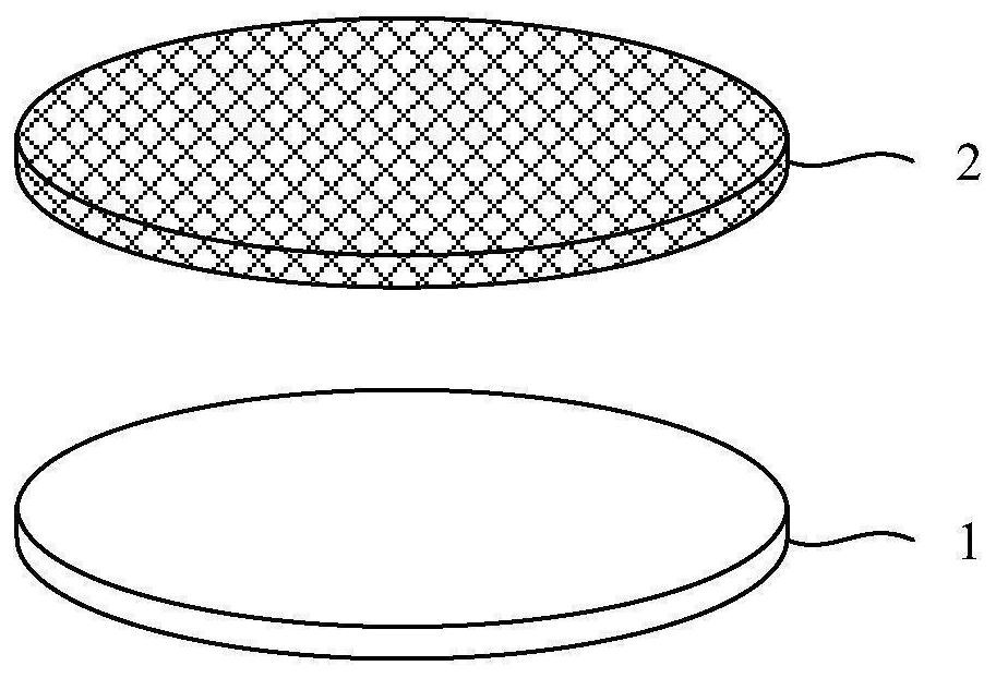
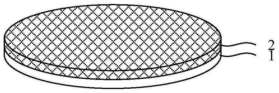
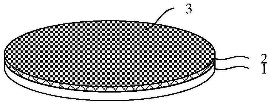
[0095] see Figure 1 to Figure 4 , performing a first bonding step: providing a carrier 1 and a first wafer 2, bonding the front side of the first wafer 2 to the carrier 1, thinning the back side of the first wafer 2, and The pads 3 are led out from the back of the first wafer 2 to form a first dicing line 4 in the first wafer 2 , and the first dicing line 4 penetrates the first wafer 1 up and down.

[0096] Specifically, such as figure 1 Shown is a schematic diagram of the carrier 1 and the first wafer 2 provided.

[0097] As an example, the first wafer 2 may be a wafer that has completed a certain process, such as a DRAM or 3D NAND storage array process integration process, a peripheral circuit (Peripheral Circuits) process integration process, etc., which may include peripheral circuits, Three-dimensional storage devices (such as 3D NAND core array (Core Array)), CMOS ima...

Embodiment 2

[0128] This embodiment adopts basically the same technical solution as that of Embodiment 1, the difference is that, in Embodiment 1, two wafers are bonded, and in this embodiment, the number of bonded wafer layers is more.

[0129] As an example, such as Figure 1 to Figure 8 As shown, the first bonding step and the second bonding step are basically the same as those in Embodiment 1. Then, before the splitting step, the second bonding step is repeated at least once to obtain a bonding structure in which at least three layers of wafers are stacked sequentially from bottom to top. After backside thinning and external wiring (Pad-out) are performed on the last bonded wafer, the splitting step basically the same as that in Embodiment 1 is performed.

[0130] As an example, a third wafer, a fourth wafer, a fifth wafer, etc. can be sequentially bonded on the second wafer, and the specific number of bonded wafers can be adjusted as required, and should not be overly limited here. ...

Embodiment 3

[0133] This embodiment provides a semiconductor structure, which is manufactured by using the multi-wafer dicing method described in Embodiment 1 or Embodiment 2. The semiconductor structure includes, but is not limited to, a three-dimensional memory device, a CMOS image sensor, and the like.

[0134] In summary, the multi-wafer dicing method formed by hybrid process bonding of the present invention and the method of thinning and cutting after changing the semiconductor structure of the current wafer bonding, reserve grooves on the temporary carrier, and place each wafer After the back of the bonded wafer is thinned to form a bonding pad, it is cut (but not split), and after the bonding and wiring of all the wafers are completed, it is split (scribed) at one time, so as to realize multi-piece stacked silicon wafers. Cutting and scribing at the circular level. The invention takes into account the advantages of mechanical cutting, laser cutting and plasma dry etching cutting, r...


PUM


Abstract

The invention provides a multi-wafer dicing method and a semiconductor structure, the method comprising the following steps: a first bonding step: providing a carrier and a first wafer, bonding the two, and thinning the back side of the first wafer Lead out the pads on the back side of the first wafer to form the first dicing line in the first wafer; the second bonding step: provide a second wafer with pads on the front side, and connect the front side of the second wafer to the The back side of the first wafer is bonded, the back side of the second wafer is thinned, and the pad is drawn out on the back side of the second wafer to form a second cutting line in the second wafer; splitting step: split the carrier along the cutting line Open to get multiple separate chips. The invention can realize wafer-level cutting and dicing of multi-layer laminated silicon wafers, wherein each layer of bonded wafers is cut independently, which can reduce the risk of edge chipping, splitting, pollution or polycrystalline change, and improve production Efficiency and the yield of packaged products, and can shrink the area of ​​the dicing line to improve the utilization rate of the wafer.

Description

technical field [0001] The invention belongs to the technical field of semiconductor integrated circuits, and relates to a multi-wafer dicing method and a semiconductor structure. Background technique [0002] At present, the fabrication of multi-layer stacked devices usually involves wafer bonding and then thinning and cutting. There are currently three main methods for multi-layer wafer dicing: [0003] (1) Traditional mechanical front cutting: When the workpiece is hard and brittle, the diamond particles break the workpiece by fracturing, and then use the knife edge to remove the powder. Its relevant characteristics are as follows: [0004] Cutting speed: 5~10mm / s; [0005] Cutting line width: 40~80μm; [0006] Cutting effect: the cut marks are deep and wide, and the wafer is easy to chip and break; [0007] Heat-affected zone: large (need to introduce water cooling and cleaning steps); [0008] Residual stress: large (cutting vibration and stress lead to crushing);...

Claims


Application Information

Patent Timeline
Patent Type & Authority Patents(China)
IPC IPC(8): H01L21/78H01L21/60H01L23/488
CPCH01L21/78H01L23/488H01L24/81H01L2224/818
Inventor 肖莉红
Owner YANGTZE MEMORY TECH CO LTD
Learn More