
Compound, display panel and display device

A display panel and compound technology, which is applied in the fields of compounds, display panels and display devices, can solve the problems of affecting OLED luminous quantum efficiency, reducing component efficiency and thermal stability, and reducing exciton formation efficiency, so as to achieve suppression of electron transport performance and Reduced exciton formation efficiency, enhanced electron injection and transport capabilities, and effects of high exciton utilization

Active Publication Date: 2020-09-29
WUHAN TIANMA MICRO ELECTRONICS CO LTD
View PDF4 Cites 1 Cited by
  • Summary
  • Abstract
  • Description
  • Claims
  • Application Information

AI Technical Summary

Problems solved by technology

However, the commonly used HTM has a higher hole-transporting ability, while the electron-transporting ability of ETM is much lower, resulting in more holes than electrons migrating to the light-emitting layer, making the electrons and holes of the entire device The mobility is unbalanced, and the exciton formation efficiency is greatly reduced, which affects the luminous quantum efficiency of OLEDs
[0004] In addition, the glass transition temperature (Tg) of the currently used ETM is low (<85°C), which causes Joule heat to be generated during OLED operation, resulting in molecular degradation and molecular structure changes, which will reduce the efficiency of the module and thermal stability, but also shortens component life

Method used

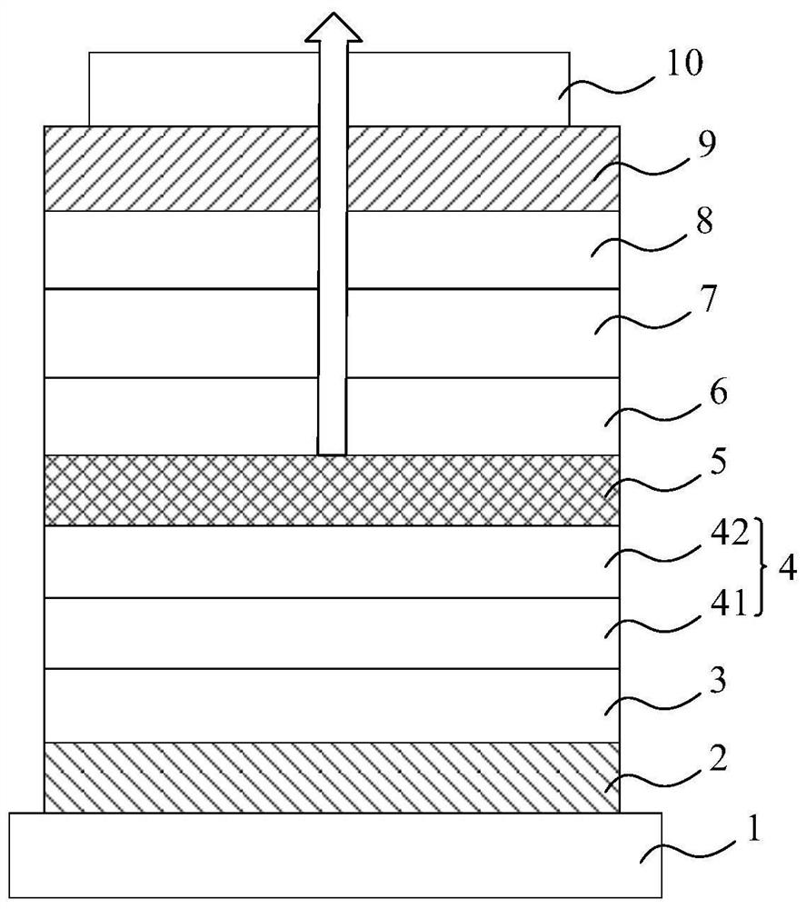

Image

  • Compound, display panel and display device
  • Compound, display panel and display device
  • Compound, display panel and display device

Examples


Embodiment 1

[0130] Embodiment 1: the synthesis of compound H-25

[0131] (one)

[0132] Under nitrogen atmosphere, add re-2 (5mmol) to 100mL anhydrous THF, stir at -78°C for 10min, wait for the reaction solution to cool down, add 1.6M n-BuLi (5mmol) dropwise, and wait until the dropwise addition is complete, React at -78°C for 2h; dissolve re-1 (5mmol) into 50mL of anhydrous THF solution, and then drop it into the low-temperature reaction solution with a syringe. After the addition is complete, continue the reaction at low temperature for 1h, and then warm up to room temperature for reaction 6h. After the reaction is completed, add a small amount of water to quench, add water and dichloromethane to extract, collect the organic phase and dry it with anhydrous sodium sulfate, collect the filtrate by suction filtration, and spin off the solvent to obtain a crude product.

[0133] Add the above crude product into 80mL acetic acid under nitrogen, stir and heat, react at 120°C for 2h, then ...

Embodiment 2

[0139] Embodiment 2: the synthesis of compound H-50

[0140] (two)

[0141] The preparation method was similar to that of Example 1, except that re-3 in step (2) of Example 1 was replaced with an equimolar amount of re-4 to finally obtain the target compound H-50 (yield 78%).

[0142] LC-MS: m / z: Calculated: C58H36N4OS: 837.00, Found: 836.79.

[0143] Elemental analysis results of the compound: calculated value: C58H36N4OS (%): C 83.23, H 4.34, N 6.69; test value: C 83.24, H 4.35, N 6.70.

Embodiment 3

[0144] Embodiment 3: the synthesis of compound H-53

[0145] (two)

[0146] The preparation method was similar to that of Example 1, except that re-3 in step (2) of Example 1 was replaced with an equimolar amount of re-5 to finally obtain the target compound H-53 (yield 75%).

[0147] LC-MS: m / z: Calculated: C56H34N6OS: 838.97, Found: 838.61.

[0148] Compound elemental analysis results: calculated value: C56H34N6OS (%): C 80.17, H 4.08, N 10.02; test value: C 80.18, H 4.07, N 10.04.


PUM

PropertyMeasurementUnit
Thicknessaaaaaaaaaa
Luminous efficiencyaaaaaaaaaa

Abstract

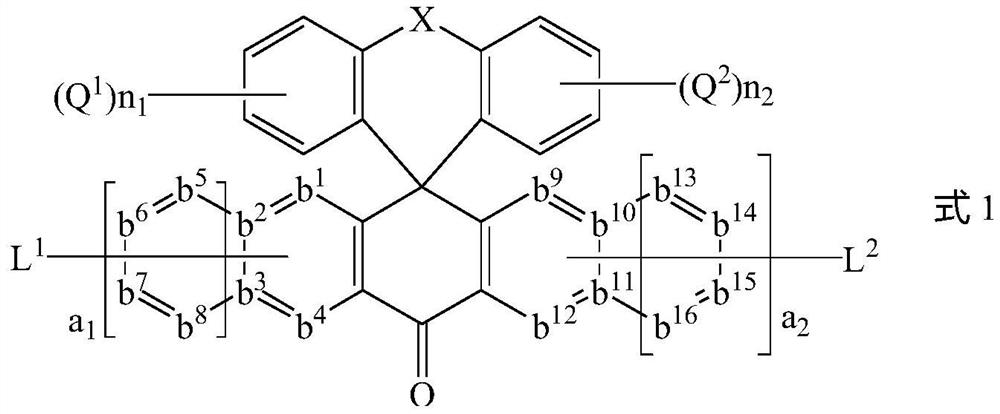
The invention discloses a compound, a display panel and a display device. The compound has a structure as shown in formula 1; and in the formula 1, X, a1, a2, b<1> to b<16>, L<1>, L<2>, Q<1>, Q<2>, n1and n2 are respectively defined in the specification. The compound provided by the invention can be used for the display panel and the display device.

Description

technical field [0001] The invention belongs to the technical field of organic luminescence, and in particular relates to a compound, a display panel and a display device. Background technique [0002] An organic light emitting diode (OLED) is a self-luminous device that utilizes an organic thin film layer to generate electroluminescent light. Specifically, under the drive of an external electric field, OLED injects holes and electrons from the anode and cathode respectively; the holes and electrons migrate to the light-emitting layer respectively and combine in the organic light-emitting material to generate excitons; the excitons in the excited state can be The form of light releases energy back to a stable ground state, producing visible light. Choosing different luminescent materials can produce different colors of emitted light to meet different color requirements. [0003] Typically, a hole transport layer (HTL) comprising a hole transport material (HTM) and an elect...

Claims


Application Information

Patent Timeline
IPC IPC(8): C07D335/04C07D409/04C07D409/14C07D471/04C07D413/04C07D413/14C07D519/00C07D495/10C07D311/96C07D405/14C07D405/04C07D491/107C07F9/6553C07F9/655H01L51/50H01L51/54
CPCC07D335/04C07D409/04C07D409/14C07D471/04C07D413/04C07D413/14C07D519/00C07D495/10C07D311/96C07D405/14C07D405/04C07D491/107C07F9/655372C07F9/65522H10K85/656H10K85/6565H10K85/654H10K85/6576H10K85/6574H10K85/657H10K85/6572H10K50/18H10K50/16H10K50/11
Inventor 冉佺高威牛晶华张磊代文朋
Owner WUHAN TIANMA MICRO ELECTRONICS CO LTD
Learn More