

Silicon-based patch and preparation method therefor
A silicon-based patch and patch technology, applied in other medical devices, hypodermic injection devices, needles, etc., can solve the problems of complex process, high cost, slow production, etc., and achieve the effect of simple process and low cost
- Summary
- Abstract
- Description
- Claims
- Application Information
AI Technical Summary
Problems solved by technology
Method used
Image

Examples
preparation example Construction
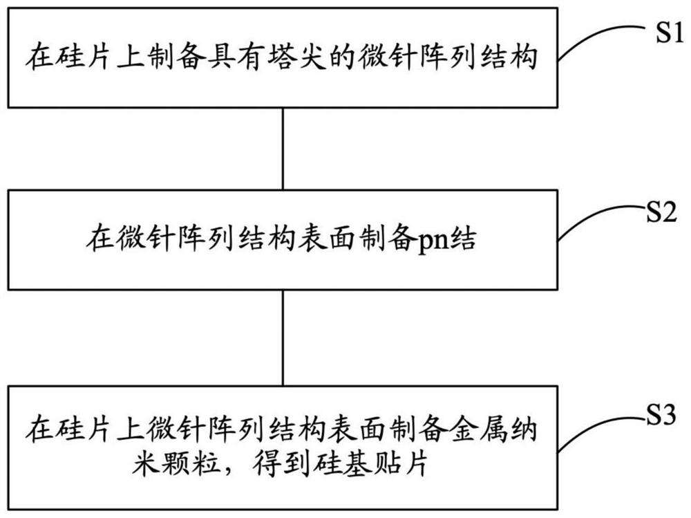
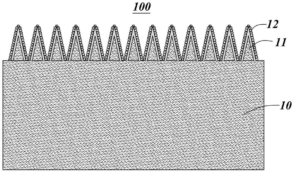
[0038] ginseng Figure 1 to Figure 3 As shown, the invention discloses a method for preparing a silicon-based patch, the method comprising:
[0039] S1. Prepare a microneedle array structure 11 with spires on the silicon wafer 10;
[0040] S2. Prepare a pn junction on the surface of the microneedle array structure 11, including an n-Si region 111 and a p-Si region 112;
[0041] S3 , preparing metal nanoparticles 12 on the surface of the microneedle array structure 11 on the silicon wafer to obtain a silicon-based patch 100 .
[0042] Further, step S1 includes:
[0043] Place the silicon wafer in an alkaline solution, and prepare a pyramid structure on the surface of the silicon wafer through a chemical etching process;
[0044] The silicon wafer is placed in an etching solution, and modified by chemical etching to form a microneedle array structure with sharp spires.
[0045] Among them, the chemical etching process is specifically:
[0046] Place the (100) crystalline si...
Embodiment 1
[0054] The preparation method of the silicon-based patch in this embodiment is as follows:
[0055] 1. Prepare a microneedle array structure with a spire on a silicon wafer.
[0056] First, an array mask is formed on the surface of the silicon wafer by steps such as pattern exposure, photoresist development, and chromium layer etching;
[0057] Then place the silicon chip of (100) crystal orientation in alkaline solution to corrode, the concentration of alkali in the alkaline solution is 5%, the reaction temperature is 70 DEG C, the reaction time is 300min, finally form the microneedle of pyramid shape on the surface of silicon chip, microneedle The needle height is 120μm, and the microneedle distribution density is about 625 / cm 2 .
[0058] 2. Prepare a pn junction on the surface of the microneedle array structure.
[0059] A pn junction is prepared on the surface of the microneedle array structure by high-temperature diffusion, and the sheet resistance of the pn junction ...
Embodiment 2
[0064] The preparation method of the silicon-based patch in this embodiment is as follows:
[0065] 1. Prepare a microneedle array structure with a spire on a silicon wafer.
[0066] First, an array mask is formed on the surface of the silicon wafer by steps such as pattern exposure, photoresist development, and chromium layer etching;
[0067] Then place the silicon wafer with (100) crystal orientation in an alkaline solution to etch, the alkali concentration in the alkaline solution is 5%, the reaction temperature is 70° C., the reaction time is 30 minutes, and the size of the pyramid structure formed on the surface of the silicon wafer is 80 μm;
[0068] Then, the above-mentioned pyramid structure is corroded by 0.5% lye containing additives, and finally a microneedle array structure with sharp spires is formed on the surface of the silicon wafer. The size of the microneedles with sharp spires is 50um, and the distribution density of the microneedles is about 625 piece / cm ...
PUM
| Property | Measurement | Unit |
|---|---|---|
| Size | aaaaa | aaaaa |
Abstract
Description
Claims
Application Information