Perovskite solar cell without electron transport layer and hole transport layer and manufacturing method

A technology of hole-transport layer and electron-transport layer, which is applied in the field of perovskite solar cells without electron-transport layer and hole-transport layer and its production, can solve the problems of exacerbating device degradation, achieve dark current density reduction, and achieve good photoelectric conversion effect, the effect of improving reliability and stability

Pending Publication Date: 2020-10-16
XIDIAN UNIV
View PDF2 Cites 5 Cited by
  • Summary
  • Abstract
  • Description
  • Claims
  • Application Information

AI Technical Summary

Problems solved by technology

In addition, the atoms in the metal electrodes of the device tend to diffuse to the organic-inorganic hybrid lead halide perovskite film

Method used


Image

  • Perovskite solar cell without electron transport layer and hole transport layer and manufacturing method
  • Perovskite solar cell without electron transport layer and hole transport layer and manufacturing method
  • Perovskite solar cell without electron transport layer and hole transport layer and manufacturing method

Examples


Embodiment 1

[0039] (1) Clean the FTO substrate: Put the FTO substrate into Decon-90 aqueous solution, deionized water, acetone, alcohol and deionized water for 15 minutes for ultrasonic cleaning;

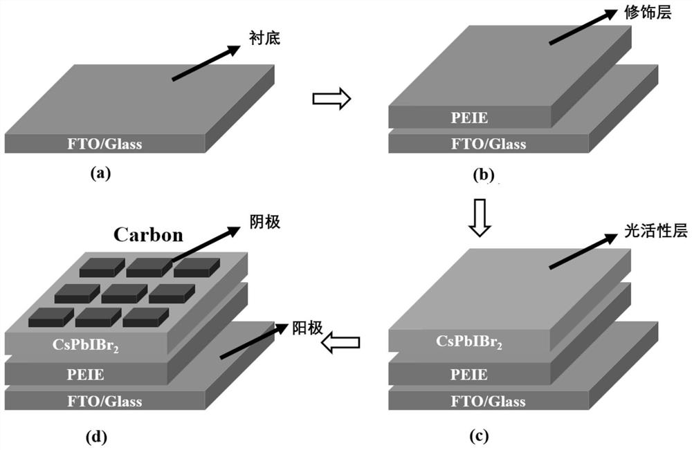
[0040] (2) UV-O 3 Treatment of FTO substrate: place the cleaned FTO substrate in UV-zone for 30min. like figure 1 as shown in (a);

[0041] (3) Preparation of PEIE modification layer: PEIE deionized aqueous solution was directly spin-coated on the FTO substrate at a speed of 3000 rpm in the air environment, and placed on a hot stage at a constant temperature of 250° C. in the air environment for annealing for 20 min. PEIE deionized water solution is prepared by dissolving a certain amount of PEIE solution in deionized water. Wherein the concentration of PEIE solution is 4mg / mL such as figure 1 as shown in (b);

[0042] (4) Preparation of CsPbIBr 2 Thin film: take PbBr with a mass ratio of 330mg 2 Solid, 27.8 mg of PbCl 2 Solid and 260.0mg CsI solid, dissolved in 1mL of dimethyl sulfoxid...

Embodiment 2

[0045] 1) Clean the FTO substrate: Put the FTO substrate into Decon-90 aqueous solution, deionized water, acetone, alcohol and deionized water for 20 minutes for ultrasonic cleaning;

[0046] 2) UV-O 3 Treatment of FTO substrates: place the cleaned FTO substrates in a UV-zone for 35 minutes.

[0047] like figure 1 as shown in (a);

[0048] 3) Preparation of PEIE modification layer: PEIE deionized aqueous solution was directly spin-coated on the FTO substrate at a speed of 3000 rpm in the air environment, and placed on a hot stage at a constant temperature of 250° C. in the air environment for annealing for 20 minutes. PEIE deionized water solution is prepared by dissolving a certain amount of PEIE solution in deionized water. Wherein the concentration of PEIE solution is 8mg / mL such as figure 1 as shown in (b);

[0049] 4) Preparation of CsPbIBr 2 Film: take 330mg of PbBr 2 Solid, 27.8 mg of PbCl 2 Solid and 260.0mg CsI solid, dissolved in 1mL of dimethyl sulfoxide sol...

Embodiment 3

[0052] 1) Clean the FTO substrate: put the FTO substrate into Decon-90 aqueous solution, deionized water, acetone, alcohol, and deionized water for 15 minutes for ultrasonic cleaning;

[0053] 2) UV-O 3 Treat the FTO substrate: place the cleaned FTO substrate in the UV-zone for 40 minutes.

[0054] like figure 1 as shown in (a);

[0055] 3) Preparation of PEIE modification layer: PEIE deionized aqueous solution was directly spin-coated on the FTO substrate at a speed of 3000 rpm in the air environment, and placed on a hot stage at a constant temperature of 250° C. in the air environment for annealing for 20 minutes. PEIE deionized water solution is prepared by dissolving a certain amount of PEIE solution in deionized water. Wherein the concentration of PEIE solution is 12mg / mL such as figure 1 as shown in (b);

[0056] 4) Preparation of CsPbIBr 2 Thin film: take PbBr with a mass ratio of 330mg 2 Solid, 27.8 mg of PbCl 2 Solid and 260.0mg of CsI solid, dissolved in 1mL ...


PUM

PropertyMeasurementUnit
Thicknessaaaaaaaaaa
Thicknessaaaaaaaaaa
Thicknessaaaaaaaaaa

Abstract

The invention discloses a perovskite solar cell without an electron transport layer and a hole transport layer and a manufacturing method. The perovskite solar cell comprises an FTO substrate, an FTOelectrode, a PEIE modification layer and a perovskite photoactive layer which are sequentially distributed from bottom to top, wherein an anode is arranged above the perovskite photoactive layer, anda cathode is arranged above the FTO substrate. In the structure, the use of an organic-inorganic hybrid lead halide perovskite material, an organic hole transport layer material and an expensive metalelectrode is avoided, and meanwhile, an electron transport layer is abandoned; the PEIE material is deposited on the FTO electrode; according to the method, a monomolecular layer can be introduced tothe surface, and an interface dipole is formed between the FTO electrode and the perovskite photoactive layer, so that the work function of the surface of the FTO electrode is reduced, and the energylevels of the FTO electrode and the CsPbIBr2 photoactive layer are more matched. Recombination between photon-generated carriers is greatly inhibited. And meanwhile, the open-circuit voltage and thefilling coefficient of the device are obviously improved.

Description

technical field [0001] The invention belongs to a perovskite solar cell, in particular to a simple and low-cost perovskite solar cell without an electron transport layer and a hole transport layer, and avoids the use of organic-inorganic hybrid lead with poor stability in its structure Halide perovskite materials, organic hole transport layer materials, expensive metal electrodes, while abandoning the complex preparation process of the electron transport layer, the PEIE modification layer makes the energy level more matching. The recombination between photogenerated carriers is greatly suppressed. At the same time, the open circuit voltage and fill factor of the device are significantly improved. Background technique [0002] As a new type of semiconductor material, organic-inorganic hybrid lead halide perovskite has many excellent optical and electrical properties such as large absorption coefficient, adjustable band gap, long carrier diffusion length, high mobility, and l...

Claims


Application Information

Patent Timeline
IPC IPC(8): H01L31/0216H01L31/0224H01L31/032H01L31/06H01L31/18
CPCH01L31/02167H01L31/022425H01L31/032H01L31/06H01L31/18Y02E10/50Y02P70/50
Inventor 朱卫东张泽阳张春福陈大正张进成郝跃
Owner XIDIAN UNIV
Why Eureka
Try Eureka