

Thin film crystalline silicon perovskite heterojunction solar cell and preparation method thereof
A solar cell, perovskite technology, applied in circuits, photovoltaic power generation, electrical components, etc., can solve problems such as photoelectric conversion performance degradation
- Summary
- Abstract
- Description
- Claims
- Application Information
AI Technical Summary
Problems solved by technology
Method used
Image

Examples
Embodiment 1
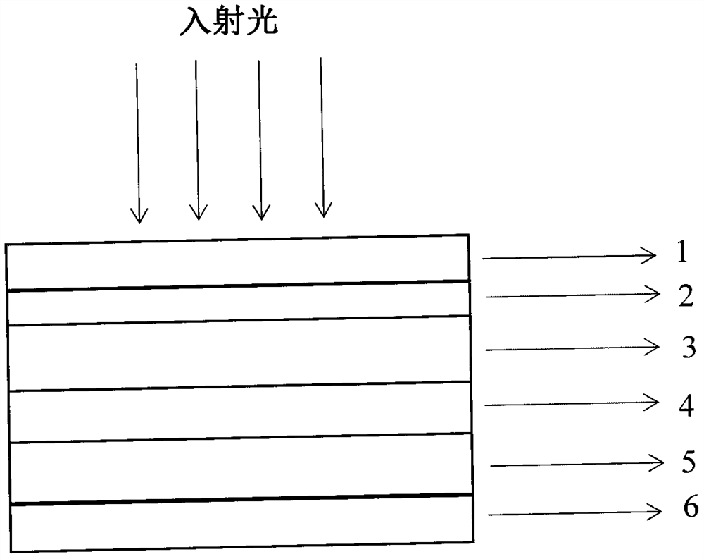
[0064] A thin-film crystalline silicon perovskite heterojunction solar cell with an electron-blocking structure layer consists of a transparent conductive substrate, a P-type thin-film crystalline silicon hole transport layer, an electron-blocking structure layer, a perovskite light-absorbing layer, and a dense titanium dioxide. The electron blocking structure layer is between the P-type crystalline silicon thin film layer and the perovskite light absorbing layer, and is composed of P-type thin-film nickel oxide; its composition sequence is: P-type thin-film crystalline silicon space The hole transport layer is placed on the transparent conductive substrate, the electron blocking structure layer is placed on the P-type thin film crystalline silicon hole transport layer, the perovskite light absorbing layer is placed on the electron blocking structure layer, and the electron blocking layer composed of dense titanium dioxide The transport layer is placed on the perovskite light-a...
Embodiment 2
[0090] A thin-film crystalline silicon perovskite heterojunction solar cell with an electron-blocking structure layer consists of a transparent conductive substrate, a P-type thin-film crystalline silicon hole transport layer, an electron-blocking structure layer, a perovskite light-absorbing layer, and a dense titanium dioxide. The electron blocking structure layer is composed of a P-type nickel oxide film between the P-type crystalline silicon thin film layer and the perovskite light-absorbing layer; its composition sequence is: P-type thin-film crystalline silicon space The hole transport layer is placed on the transparent conductive substrate, the electron blocking structure layer is placed on the P-type thin film crystalline silicon hole transport layer, the perovskite light absorbing layer is placed on the electron blocking structure layer, and the electron blocking layer composed of dense titanium dioxide The transport layer is placed on the perovskite light-absorbing la...
PUM
| Property | Measurement | Unit |
|---|---|---|
| Thickness | aaaaa | aaaaa |
| Thickness | aaaaa | aaaaa |
| Thickness | aaaaa | aaaaa |
Abstract
Description
Claims
Application Information