

Metamaterial terahertz biosensor and production method thereof
A biosensor, terahertz technology, applied in the field of sensors, can solve the problems of low absorption rate, weakened energy, weakened resonance strength, etc.
- Summary
- Abstract
- Description
- Claims
- Application Information
AI Technical Summary
Problems solved by technology
Method used
Image

Examples
preparation example Construction
[0047] The preparation method of the above-mentioned metamaterial terahertz biosensor comprises the following steps:
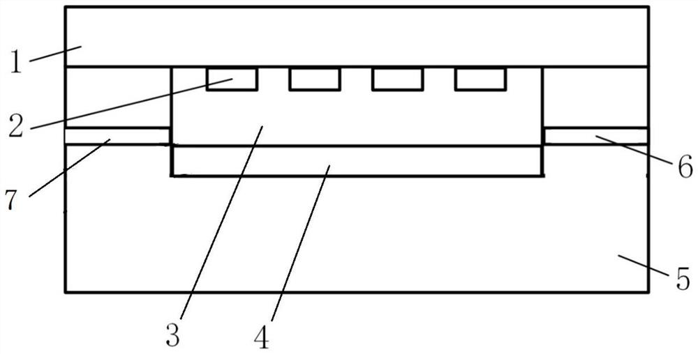
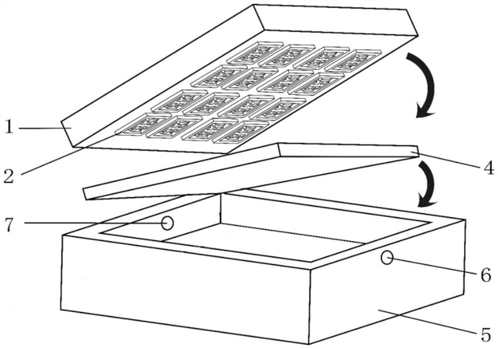
[0048] 1) Preparation of the top layer module: on the dielectric layer 1, the metal microstructure layer 2 is formed on the dielectric layer 1 through the processes of gluing, exposure, development, coating, and stripping to obtain the top layer module;
[0049] 2) Preparation of the bottom module: Etch on the base layer 5 to form a groove matching the size of the top module, then layer a metal film on the bottom surface of the groove to form a metal reflective layer 4, and finally open a groove on the base layer 5 The liquid inlet 7 and the liquid outlet 6 connected by the groove obtain the bottom module;
[0050] 3) Bonding the top module and the bottom module, forming a microfluidic channel 3 between the metal microstructure layer 2 of the top module and the metal reflection layer 4 of the bottom module, to obtain the metamaterial terahertz biosensor.
[0...
Embodiment 1
[0056] by Figure 1 to Figure 3 The structure diagram shown illustrates the structure and preparation of the sensor of the present invention.
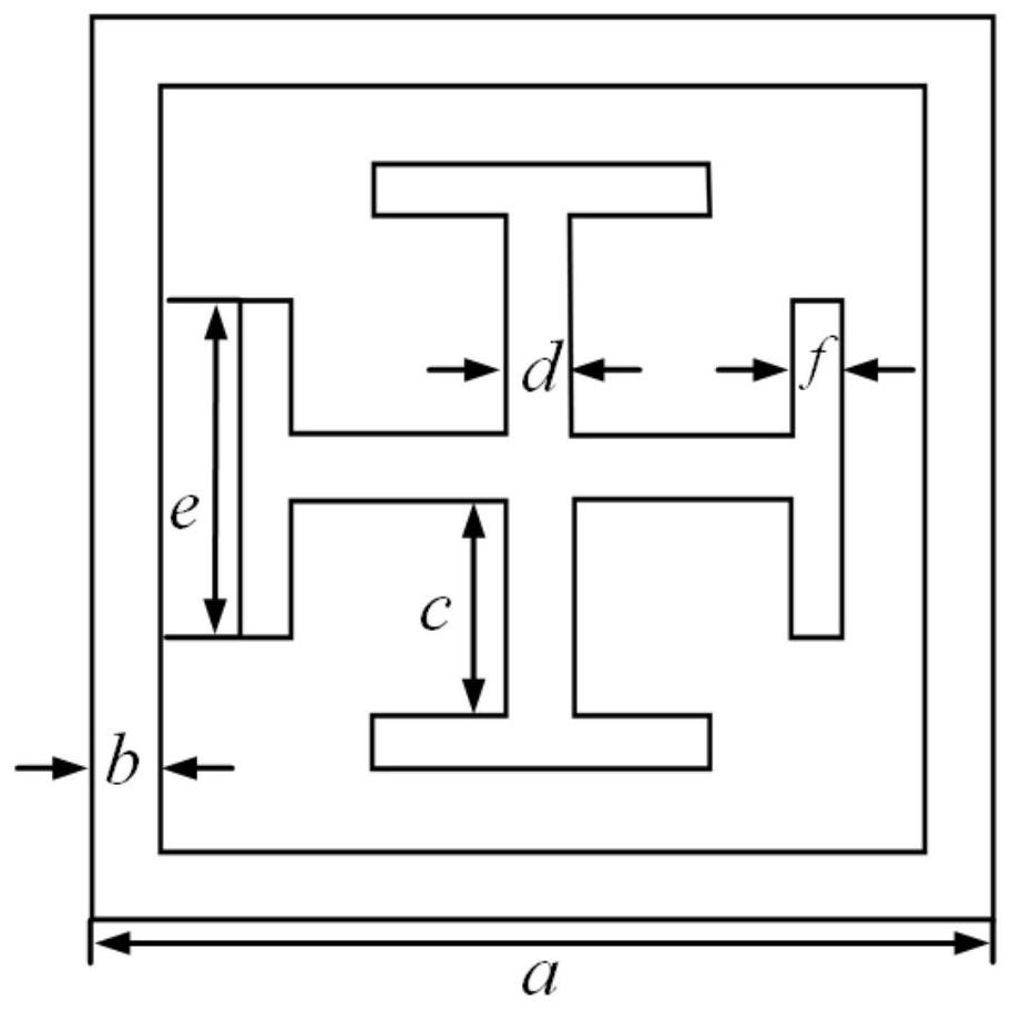
[0057] see Figure 1 to Figure 3 , the metal microstructure layer 2 is 4╳4 units periodically arranged on the dielectric layer 1, and the period of the metal microstructure layer 2 in the X-axis direction and the period in the Y-axis direction are both 120 μm. In the structure of the metal microstructure layer 2, the outer length a of the square metal ring is 108 μm, and the ring width b is 8 μm; the arm length c of the “H” metal ring in the double “H” cross metal structure is 26 μm, and the arm width d is 8 μm, the leaf length e is 40 μm, and the leaf width f is 6 μm.
[0058] The thickness of the base layer 5 is 110 μm, and its material is high resistance silicon; the thickness of the dielectric layer 1 is 6 μm, and its material is polytetrafluoroethylene; the thickness of the metal microstructure layer 2 is 0.2 μm, and its materia...
Embodiment 2
[0074] by Figure 7 The sensor structure unit of the structure shown analyzes the absorption characteristics of the sensor.
[0075] exist Figure 7 In the shown sensor structure unit, the period (Dx) of the metal microstructure layer 2 in the X-axis direction and the period (Dy) in the Y-axis direction are both 120 μm. In the structure of the metal microstructure layer 2, the outer length a of the square metal ring is 108 μm, and the ring width b is 8 μm; the arm length c of the “H” metal ring in the double “H” cross metal structure is 26 μm, and the arm width d is 8 μm, the leaf length e is 40 μm, and the leaf width f is 6 μm. The thickness of the base layer 5 is 110 μm, and its material is high-resistance silicon; the thickness of the dielectric layer 1 is 6 μm, and its material is polytetrafluoroethylene; the thickness of the metal microstructure layer 2 is 0.2 μm, and its material is silver; The reflective layer 4 has a thickness of 0.2 μm and its material is silver; t...
PUM
| Property | Measurement | Unit |
|---|---|---|
| Arm length | aaaaa | aaaaa |
| Arm width | aaaaa | aaaaa |
| Ye chang | aaaaa | aaaaa |
Abstract
Description
Claims
Application Information