AlGaN-based deep ultraviolet light emitting diode, and AlGaN epitaxial wafer and preparation method thereof

A technology for light-emitting diodes and epitaxial wafers, which is applied in electrical components, circuits, semiconductor devices, etc., and can solve the problems of great influence on internal quantum efficiency, lattice mismatch and thermal expansion coefficient differences, and lack of substrate materials.

Inactive Publication Date: 2020-11-24
CHANGCHUN INST OF OPTICS FINE MECHANICS & PHYSICS CHINESE ACAD OF SCI
5 Cites 1 Cited by

AI-Extracted Technical Summary

Problems solved by technology

[0004] At present, the main problem restricting the development of AlGaN-based deep-ultraviolet light-emitting diodes is the lack of substrate materials that match the AlGaN lattice. There are large lattice mismatches and differences in thermal expansion coefficients, resulting in more threading dislocations in the nitride films and devices grown on the substrate. These dislocations have an impact o...

Abstract

The invention relates to an AlGaN-based deep ultraviolet light emitting diode, and an AlGaN epitaxial wafer and a preparation method thereof. The AlGaN-based deep ultraviolet light emitting diode andthe AlGaN epitaxial wafer each adopt a single-layer graphical BN buffer layer as a buffer layer, and the characteristic that Van der Waals' force is adopted between layers of a single-layer BN is utilized, so that the stress in the epitaxial layer can be effectively reduced; by utilizing the characteristic that the single-layer BN and the epitaxial layer belong to III-group nitrides, better epitaxial compatibility can be achieved; furthermore, the characteristic that the pattern density and the pattern size of the patterned BN buffer layer are controllable is utilized, thus the uniformity anddensity of the nucleation center position during nitride growth can be controlled, so that the crystallization quality of the AlGaN epitaxial wafer is improved, the dislocation density of the AlGaN epitaxial wafer is reduced, and the internal quantum efficiency of the AlGaN epitaxial wafer is improved.

Application Domain

Semiconductor devices

Technology Topic

Molecular physicsMaterials science +5

Image

  • AlGaN-based deep ultraviolet light emitting diode, and AlGaN epitaxial wafer and preparation method thereof
  • AlGaN-based deep ultraviolet light emitting diode, and AlGaN epitaxial wafer and preparation method thereof
  • AlGaN-based deep ultraviolet light emitting diode, and AlGaN epitaxial wafer and preparation method thereof

Examples

  • Experimental program(1)

Example Embodiment

[0038] The following description is used to disclose the invention to enable those skilled in the art to realize the invention. The preferred embodiments in the following description are only examples, and other obvious modifications can be thought of by those skilled in the art.. The basic principles of the invention defined in the following description can be applied to other embodiments, modifications, improvements, equivalents and other technical solutions without departing from the spirit and scope of the invention.
[0039] It should be understood by those skilled in the art that in the disclosure of the present invention, the terms vertical, horizontal, upper, lower, front, back, left, right, vertical, horizontal, top, bottom, inside, and
[0040] It can be understood that the term "a" should be understood as "at least one" or "one or more", that is, in one embodiment, the number of an element may be one, while in other embodiments, the number of the element may be multiple, and the term "a" should not be understood as limiting the number.
[0041] In the description of the present invention, it should be noted that unless otherwise specified and limited, the terms "installed", "connected" and "connected" should be understood in a broad sense, for example, they can be fixedly connected, detachably connected or integrally connected; Can be mechanically connected, electrically connected or can communicate with each other; It can be directly connected or indirectly connected through an intermediate medium, and it can be the internal communication of two elements or the interaction between two elements. For those of ordinary skill in the art, the specific meanings of the above terms in the present invention can be understood according to specific situations.
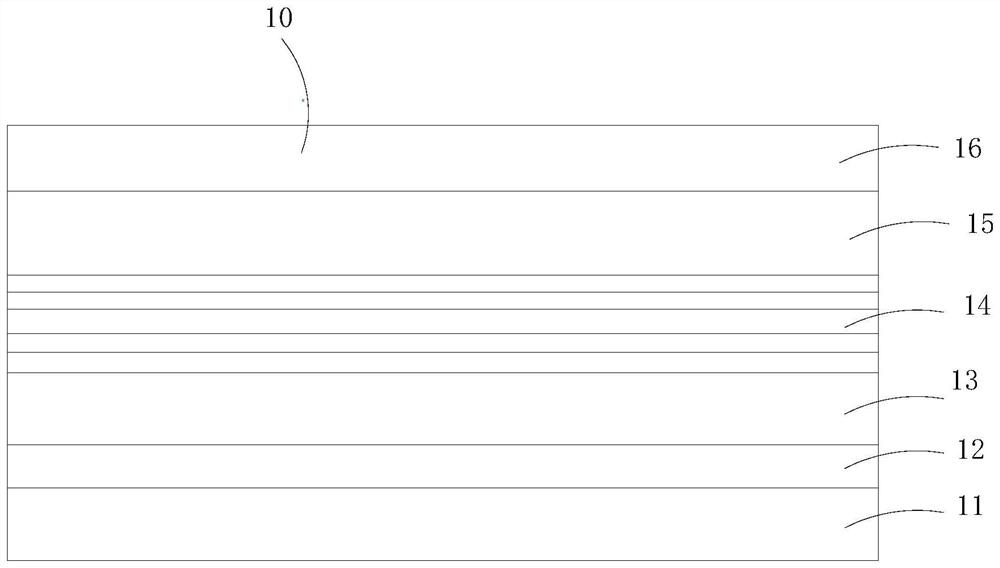
[0042] such as 1 to 3 As shown, the specific structure of the AlGaN-based deep ultraviolet light emitting diode 10 and its AlGaN epitaxial wafer according to the present invention is illustrated. such as Figure 1 As shown, the AlGaN epitaxial wafer sequentially comprises a substrate 11, a single-layer patterned BN buffer layer 12 and an AlGaN layer 13 from bottom to top, wherein the single-layer patterned BN buffer layer 12 serves as a buffer layer. The AlGaN-based deep ultraviolet light emitting diode 10 includes the AlGaN epitaxial wafer and Al grown on the AlGaN epitaxial wafer in sequence. x Ga 1-x N/Al y Ga 1-y A multi-quantum well layer 14, a p-type AlGaN layer 15, and a p-type GaN layer 16, wherein the single-layer patterned BN buffer layer 12 serves as a buffer layer.
[0043]It can be understood that because single-layer BN is a material in which atoms in layers are connected by covalent bonds and layers are connected by Van der Waals force, and two-dimensional BN is a member of the traditional III nitride semiconductor, which has good epitaxial compatibility with nitride epitaxial structures, nitride epitaxial structures prepared on two-dimensional BN buffer layers have better crystal quality and device performance. In addition, two-dimensional BN has more mature preparation technology, and has unique advantages in the regulation of crystallinity, thickness, morphology and other parameters. Compared with the covalent bonding between the traditional three-dimensional transition layer and nitride epitaxial structure, the bonding force between two-dimensional BN layers is weak, which can effectively relax the lattice mismatch at the interface. Furthermore, the patterned BN buffer layer has the advantages of controllable pattern density and pattern size, which is conducive to realizing uniform nucleation center position and controllable density during nitride growth, thereby improving the crystallization quality of the AlGaN epitaxial wafer and reducing dislocation density of the AlGaN epitaxial wafer, thereby improving the internal quantum efficiency of the AlGaN epitaxial wafer and the AlGaN-based deep ultraviolet light emitting diode 10. Therefore, by adopting the single-layer patterned BN buffer layer 12 as a buffer layer, the AlGaN epitaxial wafer can have high-quality crystallization quality and low dislocation density.
[0044] It is worth mentioning that the dislocation density of the AlGaN epitaxial wafer using the single-layer patterned BN buffer layer 12 as the buffer layer is lower than 5×10. 8 cm -2 Has an internal quantum efficiency of more than 60%, so the invention provides the AlGaN epitaxial wafer with high internal quantum efficiency.
[0045] Therefore, because the AlGaN epitaxial wafer has high internal quantum efficiency, the AlGaN epitaxial wafer can be integrated into an optoelectronic chip device, so that equipment using the optoelectronic chip device can have higher working efficiency and better working effect. The AlGaN epitaxial wafer of the present invention can be applied to an AlGaN-based deep ultraviolet light emitting diode 10 or a deep ultraviolet detector, but is not limited to it.
[0046] It is worth mentioning that the substrate 11 of the AlGaN epitaxial wafer of the present invention is any one of sapphire substrate, silicon substrate and silicon carbide substrate.
[0047] Preferably, in this preferred embodiment of the present invention, the AlGaN epitaxial wafer adopts a sapphire substrate as the substrate 11, and the crystal plane index of the sapphire substrate is (001) plane. Because the production technology of the sapphire substrate is mature, the device quality is good, the stability of the sapphire substrate is good, and it is suitable for high-temperature growth. In addition, the mechanical strength of the sapphire substrate is high, and it is easy to handle and clean. Therefore, the present invention preferably adopts the sapphire substrate as the substrate 11.
[0048] Furthermore, the single-layer patterned BN buffer layer 12 can be directly grown on the surface of the substrate 11 by chemical vapor deposition (CVD) or physical vapor deposition (PVD). In some embodiments of the present invention, the single-layer patterned BN buffer layer 12 can be grown by chemical vapor deposition (CVD) or physical vapor deposition (PVD) and then transferred to the surface of the substrate 11.
[0049] Preferably, in this preferred embodiment of the present invention, the single-layer patterned BN buffer layer 12 is directly grown and formed on the surface of the substrate 11 by chemical vapor deposition (CVD) or physical vapor deposition (PVD), so as to avoid the complicated operation of the transfer process and the contamination of the single-layer patterned BN buffer layer 12 during the transfer process.
[0050] It is worth mentioning that the formation mode of the single-layer patterned BN buffer layer 12 is as follows: firstly, a single-layer patterned BN buffer layer is grown on the surface of the sapphire substrate 11 by chemical vapor deposition (CVD) or physical vapor deposition (PVD), and secondly, a pattern is etched on the surface of the single-layer patterned BN buffer layer by ion beam etching, that is, photolithography, so as to form the single-layer patterned BN buffer layer 12.
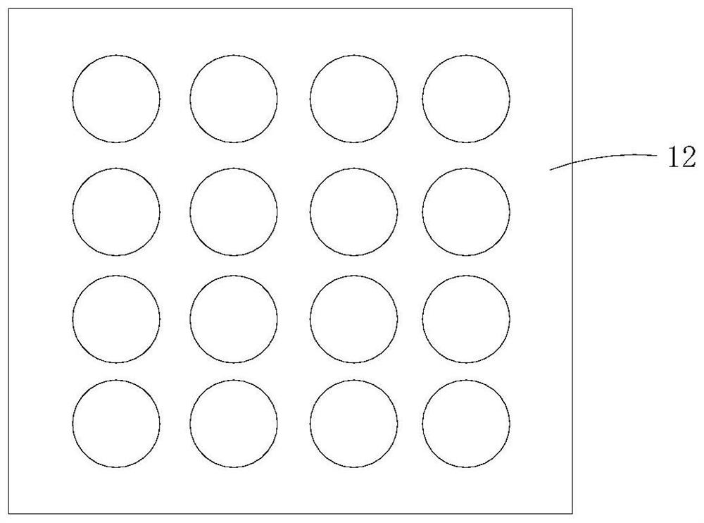
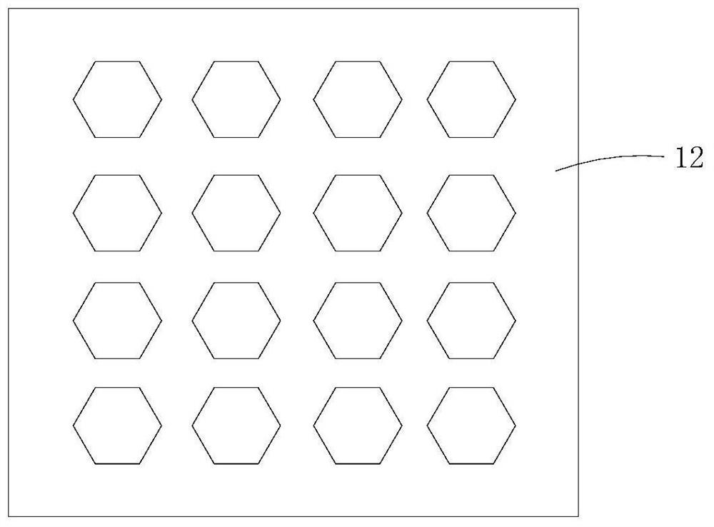
[0051] such as Figure 2 and Figure 3 As shown, the pattern shape of the single-layer patterned BN buffer layer 12 is clarified, and the pattern of the single-layer patterned BN buffer layer 12 is circular or hexagonal, that is, the pattern etched on the surface of the single-layer patterned BN buffer layer during ion beam etching is circular or hexagonal.
[0052] It should be understood that in some embodiments of the present invention, the pattern of the single-layer patterned BN buffer layer 12 may be triangular, quadrilateral, pentagonal, etc., and the present invention is not limited to the pattern shape of the single-layer patterned BN buffer layer 12.
[0053] It can be understood that when the single-layer patterned BN buffer layer 12 is obtained by ion beam etching, the pattern shape, size and density of the single-layer patterned BN buffer layer 12 can be effectively controlled, which is beneficial to realize uniform nucleation center position and controllable density during nitride growth on the surface of the single-layer patterned BN buffer layer 12. That is, it is beneficial to ensure the uniformity of the N-type AlGaN layer 13 formed on the surface of the single-layer patterned BN buffer layer 12, and further to improve the crystallization quality of the AlGaN epitaxial wafer and reduce the dislocation density of the epitaxial layer, thus improving the internal quantum efficiency of optoelectronic chip devices using the AlGaN epitaxial wafer.
[0054] It is worth mentioning that in this embodiment of the invention, the Al x Ga 1-x N/Al y Ga 1-y The Al component content x in the n quantum well layer 14 is less than y, and the Al x Ga 1-x N/Al y Ga 1-y In the n quantum well layer 14, Al x Ga 1-x Is n-well layer, Al y Ga 1-y Is n barrier layer, and the content of Al component is 0≤x
[0055] In addition, it is also worth mentioning that the Al x Ga 1-x N/Al y Ga 1-y The n-quantum well layer 14 is used as an active region, and the n-quantum well layer is formed in the Al x Ga 1-x N/Al y Ga 1-y The active region of that n quantum well lay 14 deposits p-AlGaN materiAl on the al. x Ga 1-x N/Al y Ga 1-y A p-type AlGaN layer 15 is formed on the n-quantum well layer 14.
[0056] Particularly, the p-type AlGaN layer 15 is Al. m Ga 1-m The vAlue range of n and al component content m is: y
[0057] To sum up, the present invention provides an AlGaN-based deep ultraviolet light emitting diode 10, which includes the AlGaN epitaxial wafer.
[0058]It is worth mentioning that the existing patents on nitride growth mainly focus on the use of van der Waals force between graphene layers to modulate the stress generated in the subsequent nitride growth process. For example, the patent with application number of 201710192463.6 provides a gallium nitride film and its preparation method, a graphene film and its preparation method. By sequentially forming a graphene catalytic layer with a first pore structure and a graphene mask layer with a second pore structure on the gallium nitride buffer layer, and then epitaxially growing the gallium nitride layer on the surface of the graphene mask layer and the surface of the gallium nitride buffer layer exposed in the pores of the graphene mask layer, the film forming quality of the gallium nitride film and the stability of the graphene film are improved. However, this method has complex reaction conditions and steps, high requirements for equipment, and high cost at present. Therefore, the present invention provides a new preparation method of the AlGaN-based deep ultraviolet light emitting diode 10.
[0059] such as Figure 4 As shown, the present invention also provides a preparation method of AlGaN-based deep ultraviolet light emitting diode 10, which includes the following steps:
[0060] (S1) selecting a substrate 11;
[0061] (S2) forming a single BN buffer layer on the surface of the substrate 11;
[0062] (S3) etching a pattern on the single-layer BN buffer layer to form a single-layer patterned BN buffer layer 12;
[0063] (S4) epitaxially growing an n-type AlGaN layer 13 on the single-layer patterned BN buffer layer 12;
[0064] (S5) epitaxiAlly growing al on the n-type AlGaN layer 13 x Ga 1-x N/Al y Ga 1-y The n-quantum well layer 14, the Al x Ga 1-x N/Al y Ga 1-y The n-quantum well layer 14 serves as an active region; and
[0065] (S6) in the Al x Ga 1-x N/Al y Ga 1-y P-AlGaN materiAl is deposite on that active region of the n-quantum well layer 14, so that the al x Ga 1-x N/Al y Ga 1-y A p-type AlGaN layer 15 is formed on the n-quantum well layer 14.
[0066] It can be understood that the preparation method of the AlGaN-based deep ultraviolet light emitting diode 10 of the present invention mainly uses the single-layer h-BN with complete structure and C-axis orientation growth as the buffer layer, and the single-layer h-BN buffer layer is patterned to form the single-layer patterned BN buffer layer 12, so that the pattern of the single-layer patterned BN buffer layer 12 can be used as the nucleation site for subsequent growth. Therefore, Based on the controllability of the pattern shape, size and density of the patterned etching of the single-layer patterned BN buffer layer 12, the uniformity of the nucleation center position and the controllability of the density of nitride growth on the surface of the single-layer patterned BN buffer layer 12 are formed. In other words, the invention can adjust the uniformity and density of nitride growth on the surface of the single-layer patterned BN buffer layer 12 by changing the pattern shape, size and density of the surface of the single-layer patterned BN buffer layer 12. Therefore, the invention can adjust the shape, size and density of the pattern etched by the single-layer patterned BN buffer layer 12 according to the subsequent nitride growth requirements.
[0067] It is worth mentioning that in the step (S1), the substrate 11 is any one of sapphire substrate, silicon substrate and silicon carbide substrate. Preferably, in this preferred embodiment of the present invention, the sapphire substrate is selected as the substrate 11.
[0068] In addition, it is also worth mentioning that in the step (S2), the single BN buffer layer is directly grown on the surface of the substrate 11 by chemical vapor deposition or physical vapor deposition. In some embodiments of the present invention, the single BN buffer layer can be grown by chemical vapor deposition or physical vapor deposition, and then transferred to the surface of the substrate 11.
[0069] Particularly, in the step (S3), an ion beam etching method is used to etch a pattern on the single BN buffer layer.
[0070] Optionally, the pattern of the single-layer patterned BN buffer layer 12 is circular or hexagonal.
[0071] It is worth mentioning that the Al x Ga 1-x N/Al y Ga 1-y The Al component content x in the n quantum well layer 14 is less than y, and the Al x Ga 1-x N/Al y Ga 1-y In the n quantum well layer 14, Al x Ga 1-x Is n-well layer, Al y Ga 1-y Is n barrier layer, and the content of Al component is 0≤x
[0072] Particularly, the p-type AlGaN layer 15 is Al. m Ga 1-m The vAlue range of n and al component content m is: y
[0073] It can be understood that the AlGaN-based deep ultraviolet light emitting diode 10 of the present invention adopts the single-layer patterned BN buffer layer 12 as a buffer layer, and the stress in the epitaxial layer can be effectively reduced by utilizing the characteristic that the interlayer of the single-layer patterned BN buffer layer 12 is Van der Waals force. By using the characteristic that the single-layer patterned BN buffer layer 12 and the epitaxial layer belong to III nitride, better epitaxial compatibility can be obtained; Therefore, the AlGaN-based deep ultraviolet light emitting diode 10 of the present invention has high lattice quality and low dislocation density, thus having high internal quantum efficiency.
[0074] It is worth mentioning that, on the separated p-AlGaN material and the corresponding N-type AlGaN layer 13, the P-type region electrode and the N-type region electrode suitable for light-emitting and detector devices can be respectively prepared by electron beam evaporation or thermal evaporation and rapid annealing.
[0075] In other words, on the basis of the preparation method of the AlGaN-based deep ultraviolet light emitting diode 10 of the present invention, optoelectronic chip devices suitable for light emission and detection respectively can be prepared by electron beam evaporation or thermal evaporation and rapid annealing.
[0076] The method of the present invention includes, but is not limited to, the above embodiments. The method of that invention can effectively improve the coincidence degree of detection and light-emitting wave band of AlGaN-based homogeneous integrated optoelectronic chip, thereby improving data conversion efficiency, increasing data transmission speed and improving device performance.
[0077] The technical features of the above embodiments can be arbitrarily combined. To make the description concise, all possible combinations of the technical features in the above embodiments are not described. However, as long as there is no contradiction between the combinations of these technical features, they should be considered as the scope of this specification.
[0078] The above examples only express the preferred embodiments of the invention, and their descriptions are more specific and detailed, but they should not be construed as limiting the scope of the invention patents. It should be pointed out that for those skilled in the art, without departing from the concept of the present invention, several modifications and improvements can be made, all of which belong to the scope of protection of the present invention. Therefore, the scope of protection of the patent of the present invention should be subject to the appended claims.

PUM

no PUM

Description & Claims & Application Information

We can also present the details of the Description, Claims and Application information to help users get a comprehensive understanding of the technical details of the patent, such as background art, summary of invention, brief description of drawings, description of embodiments, and other original content. On the other hand, users can also determine the specific scope of protection of the technology through the list of claims; as well as understand the changes in the life cycle of the technology with the presentation of the patent timeline. Login to view more.
Why Eureka
Try Eureka