Ultraviolet detector with high wavelength selectivity and manufacturing method thereof

A technology of wavelength selectivity and manufacturing method, which is applied in the field of photoelectric detection, can solve the problems of inconvenient portability, high cost, and large equipment volume, and achieve the effect of simple structure, easy preparation, and small volume

Active Publication Date: 2020-12-04
NANJING UNIV
View PDF5 Cites 0 Cited by
  • Summary
  • Abstract
  • Description
  • Claims
  • Application Information

AI Technical Summary

Problems solved by technology

Conventional semiconductor ultraviolet detectors have a wide response range to ultraviolet light with a wavelength shorter than the absorption edge, and cannot only respond to ultraviolet light in a narrow range, although existing spectrometers can detect ultraviolet light in specific bands, But its equipment is bulky, inconvenient and extremely expensive

Method used


Image

  • Ultraviolet detector with high wavelength selectivity and manufacturing method thereof
  • Ultraviolet detector with high wavelength selectivity and manufacturing method thereof
  • Ultraviolet detector with high wavelength selectivity and manufacturing method thereof

Examples


Embodiment 1

[0090] A method for fabricating a highly wavelength-selective ultraviolet detection device may comprise the steps of:

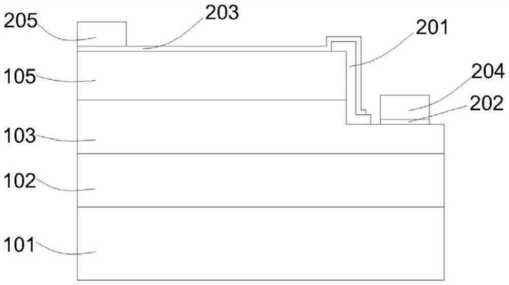
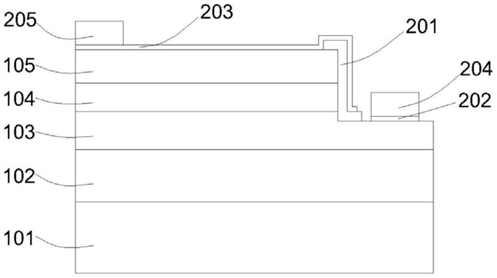
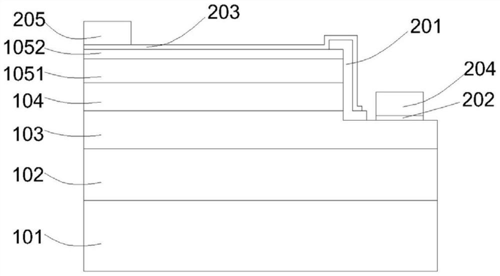
[0091] 1) GaN layer, n-GaN layer and p-GaN layer are sequentially stacked and grown on the substrate by metal organic compound chemical vapor deposition (MOCVD);

[0092] 2) Ultrasonic cleaning of the epitaxial structure obtained in step 1) with acetone, isopropanol, deionized water, etc., to remove organic impurities on the surface of the epitaxial structure, and using HCl immersion, deionized water ultrasonic treatment, etc., Remove the oxide layer on the surface of the epitaxial structure;

[0093] 3) Covering at least a partial area of ​​the surface of the p-GaN layer with a patterned mask, and removing the p-GaN layer and part of the n-GaN layer not covered by the mask in the protection area by etching, so that the part The n-GaN layer is thinned, and the surface of the thinned n-GaN layer is exposed, thereby forming a step structure between the p-GaN l...

Embodiment 2

[0100] The fabrication method of the ultraviolet detection device with high wavelength selectivity in the present embodiment is basically the same as in the embodiment 1, the difference is that the Ag-Au alloy thin film in the present embodiment is Ag 0.7 Au 0.3 Thin film, after testing, the spectral responsivity peak of the ultraviolet detection device with high wavelength selectivity obtained in Example 2 is located at 380nm, and the full width at half maximum is 80nm.

Embodiment 3

[0102] The fabrication method of the ultraviolet detection device with high wavelength selectivity in the present embodiment is basically the same as in the embodiment 1, the difference is that the Ag-Au alloy thin film in the present embodiment is Ag 0.8 Au 0.2 Thin film, after testing, the spectral responsivity peak of the ultraviolet detection device with high wavelength selectivity obtained in Example 3 is located at 360nm, and the half maximum width is 55nm.


PUM

PropertyMeasurementUnit
thicknessaaaaaaaaaa
wavelengthaaaaaaaaaa
thicknessaaaaaaaaaa

Abstract

The invention discloses an ultraviolet detection device with high wavelength selectivity and a manufacturing method thereof. The ultraviolet detector comprises a first polarity semiconductor layer, asecond polarity semiconductor layer, a first ohmic contact layer and a second ohmic contact layer, wherein the first polarity semiconductor layer is arranged on the second polarity semiconductor layer, the first ohmic contact layer forms ohmic contact with the first polarity semiconductor layer, the second ohmic contact layer forms ohmic contact with the second polarity semiconductor layer, the first ohmic contact layer comprises an Ag-Au alloy film covering the first polarity semiconductor layer, and the Ag-Au alloy film can selectively allow ultraviolet light to pass through. According to the ultraviolet detector with high wavelength selectivity provided by the embodiment of the invention, on the basis of small size and easiness in use, high-selectivity detection on ultraviolet light ofa specific waveband is realized, and meanwhile, the excellent detection performance of the ultraviolet detector is ensured by ohmic contact between the Ag-Au alloy film and the first polar semiconductor layer.

Description

technical field [0001] The invention relates to an ultraviolet detector, in particular to an ultraviolet detection device with high wavelength selectivity and a manufacturing method thereof, belonging to the technical field of photoelectric detection. Background technique [0002] Ultraviolet light can be divided into UVA (400-320nm), UVB (320-280nm) and UVC (280-100nm) according to the wavelength. Different wavelengths of ultraviolet light have different applications. For example, UVA is often used in photocuring, and UVB is often used in biomedicine. , UVC is often used for disinfection and sterilization. It is of great significance to be able to accurately measure the intensity and dose of ultraviolet radiation in specific wavebands. Conventional semiconductor ultraviolet detectors have a wide response range to ultraviolet light with a wavelength shorter than the absorption edge, and cannot only respond to ultraviolet light in a narrow range, although existing spectromet...

Claims


Application Information

Patent Timeline
Patent Type & Authority Applications(China)
IPC IPC(8): H01L31/02H01L31/103H01L31/105H01L31/18
CPCH01L31/02005H01L31/1035H01L31/105H01L31/1856H01L31/1848Y02P70/50
Inventor 周玉刚梁志斌许朝军张齐轩张荣
Owner NANJING UNIV
Why Eureka
Try Eureka