Magnetic random access memory based on III-V group narrow bandgap semiconductor

A technology of magnetic random access memory and narrow bandgap, which is applied in the direction of semiconductor devices, electric solid devices, and resistors controlled by magnetic fields, can solve the problems of difficult combination of devices, inapplicable preparation, and inability to stabilize, etc., to improve power consumption, The effect of increasing the integration of programmable and memory computing and reducing power consumption

Active Publication Date: 2020-12-08
SHANGHAI TECH UNIV
View PDF13 Cites 5 Cited by
  • Summary
  • Abstract
  • Description
  • Claims
  • Application Information

AI Technical Summary

Problems solved by technology

On the other hand, although strong spin-orbit coupling and spin-orbit moments have been found in some topological insulators and new two-dimensional material systems in recent years, most of these materials work in low temperature regions and at room temperature and in an environment exposed to air. cannot be stab...

Method used


Image

  • Magnetic random access memory based on III-V group narrow bandgap semiconductor
  • Magnetic random access memory based on III-V group narrow bandgap semiconductor

Examples


Embodiment Construction

[0018] Below in conjunction with specific embodiment, further illustrate the present invention. It should be understood that these examples are only used to illustrate the present invention and are not intended to limit the scope of the present invention. In addition, it should be understood that after reading the teachings of the present invention, those skilled in the art can make various changes or modifications to the present invention, and these equivalent forms also fall within the scope defined by the appended claims of the present application.

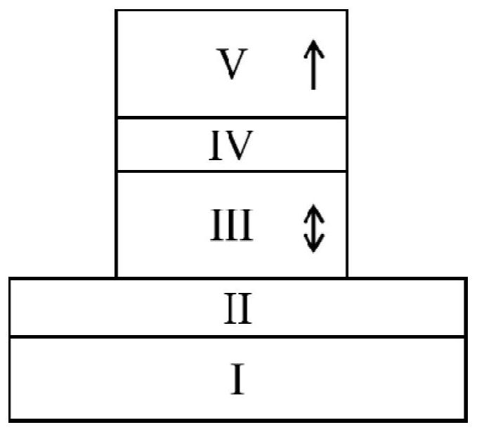
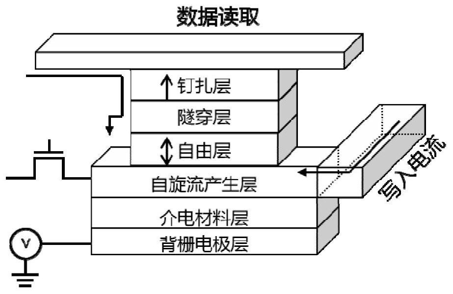
[0019] Such as figure 1 As shown, a SOT-MRAM device provided by the present invention includes a substrate wafer, a dielectric layer I, a spin-orbit torque action layer II and an MTJ structure layer.

[0020] The substrate wafer adopts N-type doped silicon or gallium arsenide wafer.

[0021] The dielectric layer I is made of cadmium telluride CdTe or zinc telluride ZnTe, with a thickness of about 1 micron. The spin-orbit tor...


PUM

PropertyMeasurementUnit
Thicknessaaaaaaaaaa
Thicknessaaaaaaaaaa
Carrier mobilityaaaaaaaaaa

Abstract

The invention relates to a magnetic random access memory based on an III-V group narrow bandgap semiconductor, the magnetic random access memory is characterized by sequentially comprising a substratewafer, a dielectric layer, a spin orbit torque acting layer and an MTJ structure layer from bottom to top, and the dielectric layer is made of a cadmium telluride CdTe or zinc telluride ZnTe material; and the spin orbit torque acting layer is made of a III-V group narrow bandgap semiconductor indium antimonide InSb or indium arsenide InAs with high mobility. The structure based on the III-V semiconductor material not only can be matched with an existing semiconductor CMOS process, but also can provide spin orbit coupling strength higher than that of a traditional heavy metal SOT material, andtherefore the problem of power consumption of device write-in current is effectively solved. In addition, the spin orbit coupling strength can be regulated and controlled by applying the back gate voltage, so that the power consumption of the device is further improved. And through electric field control, the programmable and storage integrated capability of the modified device array can be improved.

Description

technical field [0001] The invention relates to a programmable spin-orbit torque-magnetic random access memory based on a narrow band gap III-V group semiconductor heterogeneous structure. Background technique [0002] With the continuous development of the field of information technology, more and more attention has been paid to memory technology. Among them, the magnetic random access memory based on the magnetic tunnel junction has been widely concerned because of its non-volatility, high storage density, fast read and write speed, and compatibility with existing CMOS devices and processes. Traditional MRAMs use magnetic fields to read and write data, but due to the disadvantages of slow magnetic field writing speed and uncontrollable magnetic field size, the device size stagnates at 90nm and cannot be further reduced. Subsequently, the magnetic random access memory (STT-MRAM) based on spin transfer torque (STT-MRAM) uses current instead of magnetic field to perform read...

Claims


Application Information

Patent Timeline
IPC IPC(8): H01L43/10H01L43/08H01L27/22
CPCH10B61/00H10N50/85H10N50/10
Inventor 寇煦丰孙璐张勇薛丰铧
Owner SHANGHAI TECH UNIV
Why Eureka
Try Eureka