Quantum dot light-emitting diode and its preparation method

A quantum dot light-emitting and diode technology, which is applied in the manufacture of semiconductor/solid-state devices, organic semiconductor devices, electric solid-state devices, etc., can solve the problems of uneven light-emitting layer of quantum dots, interface defects of electron transport layer, affecting the light-emitting performance of devices, etc. Achieve the effect of suppressing fluorescence quenching, reducing interface defects and improving coverage

Active Publication Date: 2022-03-22
TCL CORPORATION
View PDF5 Cites 0 Cited by
  • Summary
  • Abstract
  • Description
  • Claims
  • Application Information

AI Technical Summary

Problems solved by technology

[0005] The purpose of the present invention is to provide a quantum dot light-emitting diode and its preparation method, aiming to solve the technical problem that the quantum dot light-emitting layer in the existing device is uneven, and there are interface defects between the electron transport layer and the device, thereby affecting the light-emitting performance of the device

Method used


Image

  • Quantum dot light-emitting diode and its preparation method
  • Quantum dot light-emitting diode and its preparation method
  • Quantum dot light-emitting diode and its preparation method

Examples


preparation example Construction

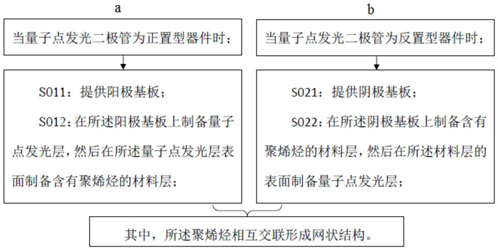
[0029] On the other hand, the embodiment of the present invention also provides a method for preparing a quantum dot light-emitting diode, including the following steps:

[0030] Such as figure 1 As shown in a, when the quantum dot light-emitting diode is a positive device,

[0031] S011: Provide anode substrate;

[0032] S012: preparing a quantum dot luminescent layer on the anode substrate, and then preparing a material layer containing polyolefin on the surface of the quantum dot luminescent layer;

[0033] or, as in figure 1 As shown in b, when the quantum dot light-emitting diode is an inverted device,

[0034] S021: Provide cathode substrate;

[0035] S022: Prepare a material layer containing polyolefin on the cathode substrate, and then prepare a quantum dot light-emitting layer on the surface of the material layer;

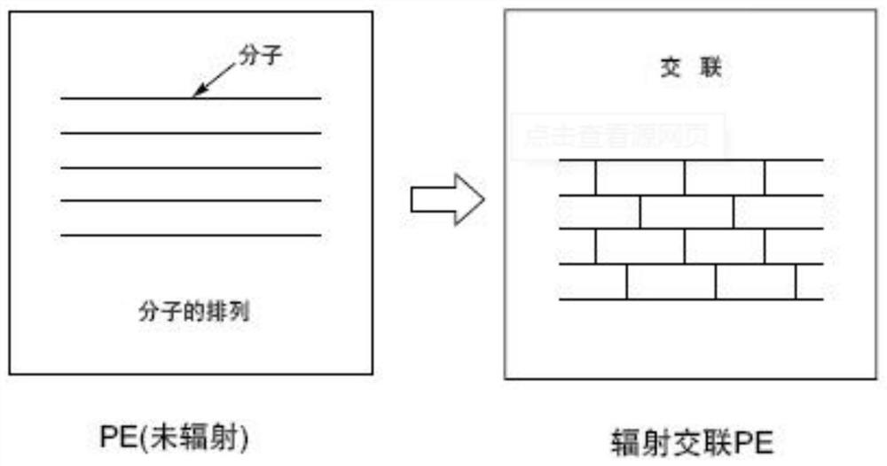
[0036] Wherein, the polyolefins are cross-linked with each other to form a network structure.

[0037] In the preparation method of the quantum dot ...

Embodiment 1

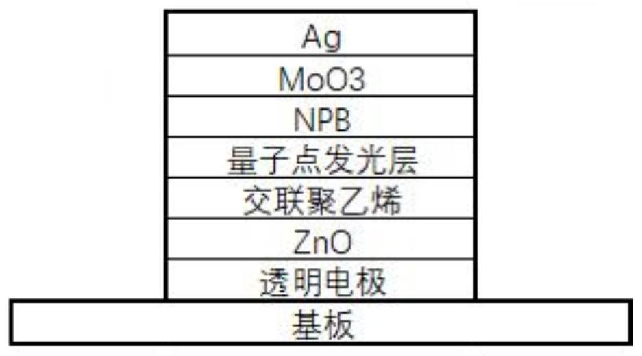
[0067] A kind of QLED device, its structure is as image 3 As shown, it includes from bottom to top: substrate, transparent electrode (cathode), ZnO electron transport layer, cross-linked polyethylene layer, quantum dot light-emitting layer, NPB hole transport layer, MoO 3 hole injection layer and Ag anode.

[0068] The preparation steps of the device are as follows:

[0069] First, the patterned ITO cathode substrate was placed in acetone, washing solution, deionized water and isopropanol in sequence for ultrasonic cleaning, and each step of ultrasonic cleaning lasted for about 15 minutes. After the ultrasound is completed, place the ITO in a clean oven to dry for later use.

[0070] After the ITO cathode substrate was dried, the ITO surface was treated with UV-ozone for 5 minutes to further remove the organic matter attached to the ITO surface and improve the work function of ITO.

[0071] Then, place the ITO cathode substrate processed in the previous step in a nitrogen ...

Embodiment 2

[0078] A kind of QLED device, its structure is as Figure 4 As shown, it includes from bottom to top: substrate, transparent electrode (cathode), ZnO electron transport layer, cross-linked polyethylene layer, quantum dot light-emitting layer, TPD hole transport layer, WO 3 Hole injection layer and Al anode.

[0079] The preparation steps of the device are as follows:

[0080]First, the patterned ITO cathode substrate was placed in acetone, washing solution, deionized water and isopropanol in sequence for ultrasonic cleaning, and each step of ultrasonic cleaning lasted for about 15 minutes. After the ultrasound is completed, place the ITO in a clean oven to dry for later use.

[0081] After the ITO substrate was dried, the ITO surface was treated with UV-ozone for 5 minutes to further remove the organic matter attached to the ITO surface and improve the work function of ITO.

[0082] Then, place the ITO cathode substrate processed in the previous step in a nitrogen atmospher...


PUM

PropertyMeasurementUnit
concentrationaaaaaaaaaa
wavelengthaaaaaaaaaa
sizeaaaaaaaaaa

Abstract

The invention belongs to the field of display technology, and in particular relates to a quantum dot light-emitting diode and a preparation method thereof. A quantum dot light-emitting diode, comprising an anode, a cathode, and a quantum dot light-emitting layer between the anode and the cathode, an electron transport layer is arranged between the cathode and the quantum dot light-emitting layer, and the electron transport A material layer containing polyolefin is arranged between the layer and the quantum dot luminescent layer, and the polyolefin is cross-linked with each other to form a network structure. In the quantum dot light-emitting diode provided by the present invention, a special material layer is arranged between the electron transport layer and the quantum dot light-emitting layer. This material layer can reduce the electron injection rate of the device cathode, adjust the distribution of quantum dot particles, and make the quantum dots The interface between the light-emitting layer and the electron-transporting layer is optimized, thereby improving the efficiency and lifetime of the device.

Description

technical field [0001] The invention belongs to the field of display technology, and in particular relates to a quantum dot light-emitting diode and a preparation method thereof. Background technique [0002] In recent years, with the rapid development of display technology, quantum dot light-emitting diodes (QLEDs) using semiconductor quantum dots (QDs) materials as the light-emitting layer have attracted extensive attention. Quantum dot light-emitting diodes have good characteristics such as high color purity, high luminous efficiency, adjustable luminous color, and stable devices, making them have broad application prospects in flat panel displays, solid-state lighting and other fields. [0003] At present, QLED usually adopts a sandwich structure, and the device includes an anode, a hole injection layer, a hole transport layer, a light-emitting layer, an electron transport layer, and a cathode; among them, the light-emitting layer is a quantum dot light-emitting layer, w...

Claims


Application Information

Patent Timeline
Patent Type & Authority Patents(China)
IPC IPC(8): H01L51/50H01L51/56
CPCH10K30/865H10K50/115H10K2102/331H10K71/00
Inventor 胡忠宇曹蔚然钱磊
Owner TCL CORPORATION
Why Eureka
Try Eureka