GaN optical sensing biosensing chip and preparation method and application thereof

A bio-sensing and light-sensing technology, applied in the field of GaN light-sensing bio-sensing chips and their preparation, can solve the problems of decreased luminescence performance, poor waterproof performance, etc., and achieve excellent biocompatibility, waterproof performance and, The effect of excellent waterproof performance

Pending Publication Date: 2021-01-12
深圳远芯光路科技有限公司
View PDF0 Cites 1 Cited by
  • Summary
  • Abstract
  • Description
  • Claims
  • Application Information

AI Technical Summary

Problems solved by technology

However, the flexible GaN ILED has poor waterproof perform

Method used


Image

  • GaN optical sensing biosensing chip and preparation method and application thereof
  • GaN optical sensing biosensing chip and preparation method and application thereof
  • GaN optical sensing biosensing chip and preparation method and application thereof

Examples


Embodiment 1

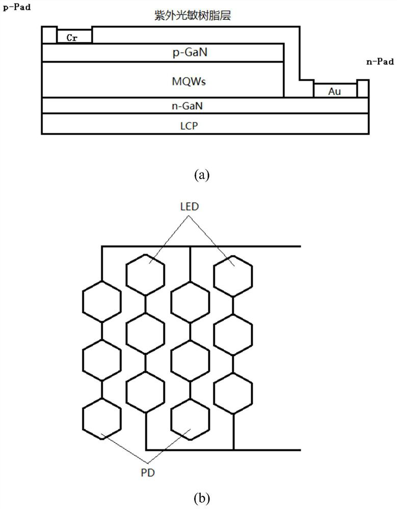
[0048] A GaN light-sensing biosensing chip as an embodiment of the present invention includes an LED array and a PD array, the LED array includes 10×10 microcolumnar LED structures connected in series, and the PD array includes 10×10 series connected The micro-columnar LED structure of the LED array, the LED array is connected to an external power supply; the micro-columnar LED structures of the LED array and the PD array sequentially include an ultraviolet photosensitive resin layer, a GaN LED epitaxial layer and a liquid crystal polymer (LCP) substrate; the said GaN LED epitaxial layer includes p-GaN layer, In x Ga 1-x N / GaN multi-dimensional quantum well, n-GaN layer, the p-GaN layer is in contact with the ultraviolet photosensitive resin layer, the n-GaN layer is in contact with the liquid crystal polymer substrate, and the GaN LED epitaxial layer Part of the n-GaN layer in the GaN LED is exposed, and the exposed n-GaN layer is contacted and connected with an n ohm contac...

Embodiment 2

[0063] A GaN light-sensing biosensing chip as an embodiment of the present invention includes a microcolumnar LED structure, the PD array includes several microcolumnar LED structures connected in series, and the LED array is connected to an external power supply; the LED array Each microcolumnar LED structure of the PD array includes an ultraviolet photosensitive resin layer, a GaN LED epitaxial layer, and a liquid crystal polymer (LCP) substrate in sequence; the GaN LED epitaxial layer includes a p-GaN layer, an In x Ga 1-x N / GaN multi-dimensional quantum well, n-GaN layer, the p-GaN layer is in contact with the ultraviolet photosensitive resin layer, the n-GaN layer is in contact with the liquid crystal polymer substrate, and the GaN LED epitaxial layer Part of the n-GaN layer in the GaN LED is exposed, and the exposed n-GaN layer is contacted and connected with an n ohm contact pad. Part of the p-GaN layer in the epitaxial layer of the GaN LED is exposed, and the exposed p...


PUM

PropertyMeasurementUnit
Center wavelengthaaaaaaaaaa
Thicknessaaaaaaaaaa

Abstract

The invention provides a GaN optical sensing biosensing chip and a preparation method and application thereof. The GaN-based optical sensing biosensing chip comprises an LED array and a PD array, theLED array comprises a plurality of micro columnar LED structures connected in series, the PD array comprises a plurality of micro columnar LED structures connected in series, and the LED array is externally connected with a power supply; each micro columnar LED structure of the LED array and the PD array sequentially comprises an ultraviolet photosensitive resin layer, a GaN LED epitaxial layer and a liquid crystal polymer substrate in sequence; the GaN LED epitaxial layer comprises a p-GaN layer, an In < x > Ga < 1 -x > N/GaN multi-dimensional quantum well and an n-GaN layer in sequence. TheGaN optical sensing biosensor chip taking the liquid crystal polymer substrate as the substrate is provided for the first time, has excellent waterproof performance, biocompatibility, mechanical performance and optical performance and excellent optical stability, and can be applied to the field of chemical and biological sensors.

Description

technical field [0001] The invention relates to the field of semiconductors, in particular to a GaN light-sensing bio-sensing chip and its preparation method and application. Background technique [0002] Light-emitting diodes (LEDs) have outstanding properties such as long-term stability, high efficiency, and strong brightness compared to traditional incandescent lamps. With these advantages, it is not only for lighting applications, but also widely used in the field of consumer electronics, such as LCD backlight unit (BLU) and large-size indoor and outdoor RGB direct display modules. In addition, since LEDs can emit light at different wavelengths, their high luminous efficiency and small size make them particularly suitable for medical applications, including body composition detectors (e.g., hemoglobin, body fat, prostate-specific antigen (PSA), and cholesterol) and therapeutic devices (e.g. disinfection, skin homeostasis, and surgical lights). In particular, flexible L...

Claims


Application Information

Patent Timeline
IPC IPC(8): H01L27/15H01L33/06H01L33/40H01L33/62H01L33/00G01N21/63G01N33/573G01N33/574G01N33/577G01N33/58
CPCH01L27/156H01L33/06H01L33/40H01L33/007H01L33/62G01N21/63G01N33/57434G01N33/57484G01N33/573G01N33/577G01N33/585H01L2933/0016H01L2933/0066G01N2333/96433
Inventor 朱玲吴懿平吕卫文祝超
Owner 深圳远芯光路科技有限公司
Why Eureka
Try Eureka