Grid mesh of cold cathode of terahertz vacuum electronic device and preparation method thereof

A vacuum electronic device, terahertz technology, applied in cold cathode manufacturing, electrode system manufacturing, electrical components and other directions, can solve the problems of flatness deformation, difficult operation, poor metal sheet strength, etc., to achieve high flatness retention and high security. quality effect

Pending Publication Date: 2021-01-29
NO 12 RES INST OF CETC
View PDF3 Cites 0 Cited by
  • Summary
  • Abstract
  • Description
  • Claims
  • Application Information

AI Technical Summary

Problems solved by technology

Metal sheets with a thickness of tens to several microns have poor strength and are difficult to handle during processing or subsequent assembly
Moreover, it is difficult for thin metal sheets to resist the thermal deformation of laser processing, and the impact of laser processing edge burrs that are difficult to completely remove compared to the size structure can no longer be ignored; similarly, flatness deformation caused by insufficient strength is difficult to guarantee high quality planar photolithography

Method used


Image

  • Grid mesh of cold cathode of terahertz vacuum electronic device and preparation method thereof
  • Grid mesh of cold cathode of terahertz vacuum electronic device and preparation method thereof
  • Grid mesh of cold cathode of terahertz vacuum electronic device and preparation method thereof

Examples


Embodiment 1

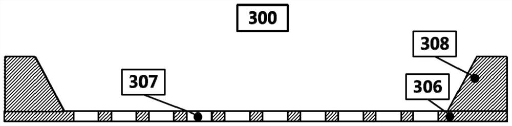
[0060] Such as image 3 As shown, the present embodiment provides a cold cathode grid 300 for a terahertz vacuum electronic device, which includes: a grid substrate 306, including a grid through-hole array 307 in the central area of ​​the grid substrate 306; a grid support The ring 308 is located on the grid substrate 306, and the two are welded together; the material of the grid substrate 306 is selected from one of copper, nickel, chromium and gold.

[0061] The thickness of the grid substrate 306 ranges from 40 microns to 5 microns depending on the frequency band of the terahertz device. In this embodiment, the exemplary thicknesses are 30 microns to 5 microns, 30 microns to 15 microns, 30 microns to 20 micron, 20 micron to 5 micron, 18 micron to 5 micron, 15 micron to 5 micron, etc., preferably 20 micron. The material of the grid substrate 306 is selected from copper, nickel, chromium, gold, etc. suitable for electroplating. In this embodiment, copper is preferred.

[00...

Embodiment 2

[0089] Repeat Example 1, the difference is that in step 4), the pattern of the photoresist mold 304 formed by photolithography is a square column, the side length is 80 microns, and the distance between each column is 10 microns, and other conditions remain unchanged. In this implementation Example The result of the grid 300 obtained is similar to that of Example 1, except that the grid transparent array hole 307 is a square hole array, and the light transmittance is 80%.

Embodiment 3

[0091] Repeat Example 1, the difference is that in step 3), the coating thickness of photoresist 303 is changed to 12 microns; in step 5), the thickness of gate electroplating layer 305 is changed to 13 microns; Electroplated layer 305 / photoresist mold 304 mixed layer grinding thickness is changed to 11 microns, polishing thickness is changed to 10 microns, and other conditions are unchanged, the result of the grid 300 obtained in this embodiment is similar to that of Example 1, the difference is that the grid The thickness of the substrate 301 is 10 micrometers.

[0092] The method of the present invention breaks through the limitation that conventional laser processing or photolithography methods can only achieve a grid with a thickness exceeding 50 microns, and can realize an ultra-thin grid with any thickness (such as 5-20 microns) in the range of 5-50 microns, and The grid plane is not easily deformed, the surface finish is better than 100nm, and the edge of the through-h...


PUM

PropertyMeasurementUnit
thicknessaaaaaaaaaa
thicknessaaaaaaaaaa
thicknessaaaaaaaaaa

Abstract

The invention discloses a grid mesh of a cold cathode of a terahertz vacuum electronic device. The grid mesh comprises a grid mesh substrate, wherein a plurality of grid electrode through hole arraysarranged in the central area of the grid mesh substrate; and a grid mesh supporting ring which is positioned on the grid mesh substrate, wherein the grid mesh supporting ring and the grid mesh substrate are welded integrally. The grid mesh can be suitable for the cold cathode of the terahertz vacuum electronic device, and the good comprehensive performance of the device can be achieved. The invention further discloses a preparation method of the terahertz vacuum electronic device cold cathode grid mesh.

Description

technical field [0001] The invention relates to the field of vacuum microelectronics. More specifically, it relates to a cold cathode grid of a terahertz vacuum electronic device and a preparation method thereof. Background technique [0002] The frequency range of traditionally defined terahertz electromagnetic radiation is 0.1-10THz. Terahertz waves have the characteristics of high radiation frequency, small divergence angle, and high signal-to-noise ratio. Therefore, terahertz technology has irreplaceable application value and development prospects in various basic research fields and applied research fields. [0003] Compared with solid-state and optical terahertz devices, the obvious advantage of terahertz vacuum electronic devices is that they have very large power capacity. Defense fields such as high-resolution imaging of space targets, guidance, and electronic countermeasures have clear application requirements. [0004] Due to the very small size of vacuum elect...

Claims


Application Information

Patent Timeline
Patent Type & Authority Applications(China)
IPC IPC(8): H01J1/304H01J9/02
CPCH01J1/304H01J9/025
Inventor 李兴辉韩攀阳杜婷姜琪杨金生蔡军冯进军
Owner NO 12 RES INST OF CETC
Why Eureka
Try Eureka