Laminate structure and method for manufacturing same, and semiconductor device

A manufacturing method and structure technology, applied in semiconductor devices, semiconductor/solid-state device manufacturing, electric solid-state devices, etc., can solve problems such as inability to perform storage operations, inability to obtain Ge atom position information, etc., and achieve excellent stability

Pending Publication Date: 2021-01-29
NAT INST OF ADVANCED IND SCI & TECH +1
View PDF15 Cites 0 Cited by
  • Summary
  • Abstract
  • Description
  • Claims
  • Application Information

AI Technical Summary

Problems solved by technology

Since the substituted Sb atoms do not participate in the phase transition required for the memory operation, if the number of Ge atoms in the GeTe alloy layer is reduced due to the substitution of Sb atoms, the change in resistance due to the phase transition Gradually getting smaller and becoming unable to perform storage actions
[0025] Second, it is reported that if a high-resolution scanning transmission electron microscope is used to observe the Ge 2 Te 2 layer with Sb 2 Te 3 layer-by-layer laminated structure, some of the Ge atoms move to a position different from the original position, and the correct positional information of the Ge atoms cannot be obtained (see Non-Patent Document 8)

Method used


Image

  • Laminate structure and method for manufacturing same, and semiconductor device
  • Laminate structure and method for manufacturing same, and semiconductor device
  • Laminate structure and method for manufacturing same, and semiconductor device

Examples


Embodiment 1

[0124]First, a sapphire substrate (manufactured by Shinko Co., Ltd.) with a thickness of 200 μm was moved to a sputtering device (manufactured by SHIBAURAMECHATRONICS Co., Ltd., 4EP-LL, equipped with three 3-inch targets). - 4 Pa, Ar film formation pressure of 0.5Pa, temperature of 25°C, and RF power of 100W, sputtering was performed using a silicon material (manufactured by Mitsubishi Materials Corporation, Si doped with B) as a target, and the sapphire substrate An amorphous silicon layer as a base layer was formed to a thickness of 40 nm.

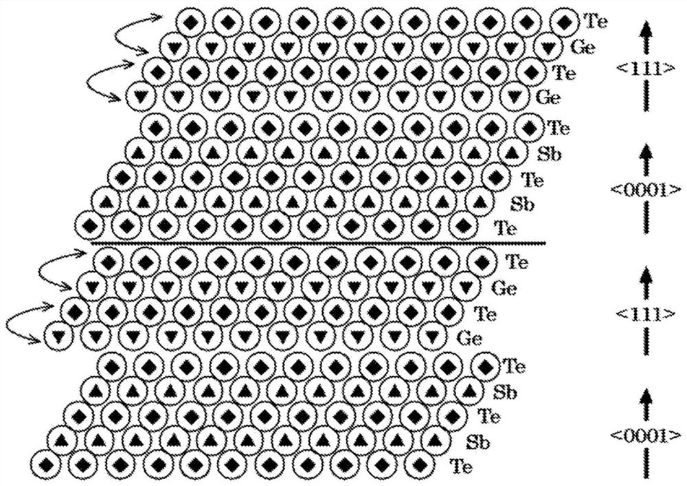
[0125] Next, maintaining the vacuum back pressure, the film formation pressure of Ar was 0.5Pa, the temperature was 25°C, and the RF power was 20W. 2 Te 3 An alloy material (manufactured by Mitsubishi Materials Corporation, purity 99.9%) was used as a target for sputtering, and Sb was formed with a thickness of 3.0 nm on the amorphous silicon layer. 2 Te 3 Alloy layer (first layer). In addition, after forming, heating at 210°C makes...

Embodiment 2

[0148] By making the target material a GeTe alloy material with S atoms added (Ge 50 Te 47 S 3 ) was changed to GeTe alloy material with added Se atoms (Ge 50 Te 47 Se 3 , manufactured by Mitsubishi Materials Corporation, purity 99.9%), except that Se atoms were added to the GeTe alloy layer, the laminated structure of Example 2 was produced in the same manner as in Example 1.

[0149] The same structural analysis as in Example 1 was carried out on the laminated structure of Example 2. As a result, the same analysis results as in Example 1 were obtained, and it was confirmed that even when Se atoms were added instead of S atoms, a stable structure was obtained. A layered structure in which atoms are arranged can suppress the diffusion of Ge atoms.

Embodiment 3

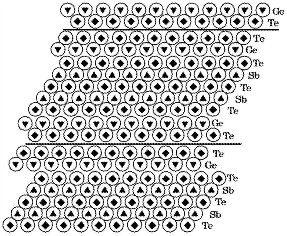
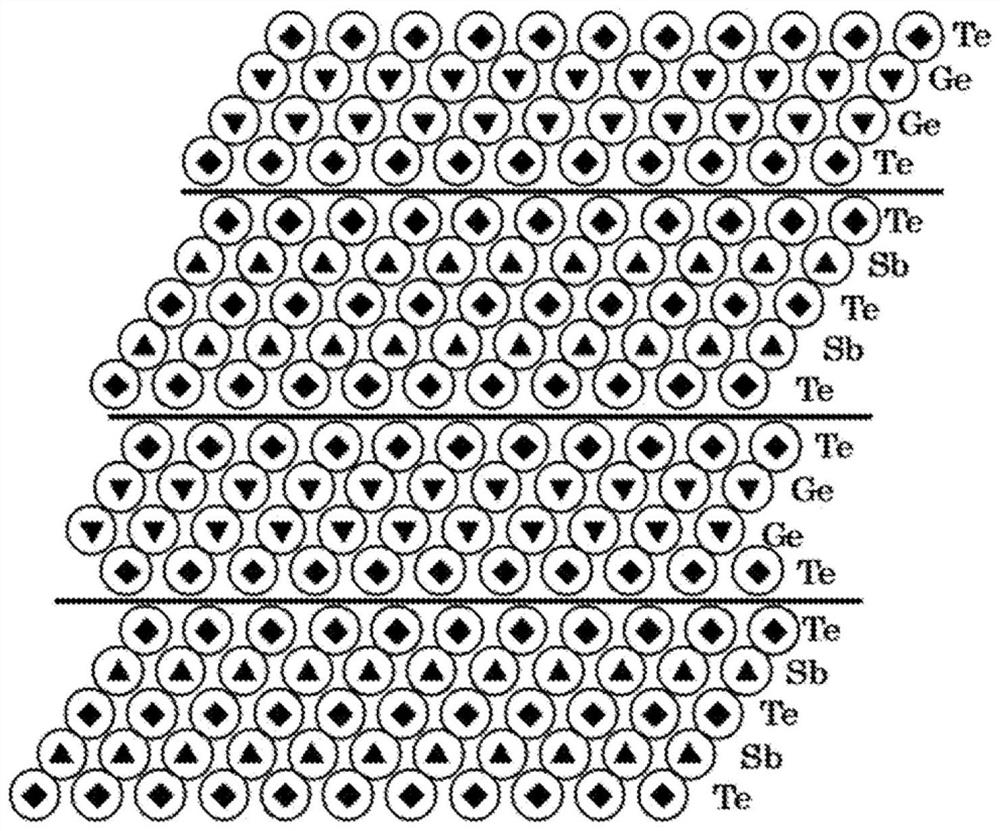
[0161] in accordance with Figure 10 With the configuration of the semiconductor device 10 shown, the semiconductor device of the third embodiment is manufactured. Hereinafter, specific production conditions will be described. also, Figure 10 It is an explanatory diagram for explaining the configuration of the semiconductor device of the third embodiment.

[0162] As the structure on the bottom surface side of the laminated structure 18, SiO formed on the silicon substrate 11 is used. 2 In the layer 12, the structure of the lower electrode of the W layer 13 and the TiN layer 14 is laminated|stacked in this order. In addition, the diameter of the TiN layer 14 was 90 nm.

[0163]Except for changing the thickness from 3.0 nm to 5.0 nm, the Sb of the first layer in the laminated structure according to Example 1 2 Te 3 alloy layer, formed on the surface of the TiN layer 14 on which the structure is formed, containing Sb 2 Te 3 Alloy base layer 15.

[0164] Next, the GeTe ...


PUM

PropertyMeasurementUnit
thicknessaaaaaaaaaa
thicknessaaaaaaaaaa
thicknessaaaaaaaaaa

Abstract

[Problem] The present invention addresses the problem of providing a laminate structure in which the atomic arrangement is highly stable, a method for manufacturing the laminate structure, and a semiconductor device in which the laminate structure is used. [Solution] This laminate structure is characterized in having an alloy layer A formed with germanium and tellurium being the main components, and an alloy layer B formed with tellurium and either antimony or bismuth being the main components, chalcogen atoms of sulfur and / or selenium being contained in the alloy layer A and / or the alloy layer B.

Description

technical field [0001] The present invention relates to a laminated structure in which two alloy layers are laminated, a method for manufacturing the laminated structure, and a semiconductor device including the laminated structure. Background technique [0002] In the existing type of phase change memory, a ternary alloy containing germanium (Ge)-antimony (Sb)-tellurium (Te) (hereinafter referred to as "GST alloy") is used, and by changing the strength and application time of the current pulse , and the recording process that achieves the transition from the amorphous phase of the high-resistance state to the crystalline phase of the low-resistance state is called setting (SET), and conversely, the recovery from the crystalline phase to the amorphous phase is called Reset (RESET) erase process. [0003] However, in the erasing process, in order to form the amorphous phase, it is necessary to temporarily inject a large current into the GST alloy to generate a temperature ab...

Claims


Application Information

Patent Timeline
Patent Type & Authority Applications(China)
IPC IPC(8): H01L21/8239C01B19/04H01L27/105H01L45/00
CPCC01B19/007H10N70/235H10N70/026H10N70/8828H10N70/826C01B19/04H10N70/011H10N70/8822H10N70/8825
Inventor 富永淳二宫田典幸鎌田善己国岛巌
Owner NAT INST OF ADVANCED IND SCI & TECH
Why Eureka
Try Eureka