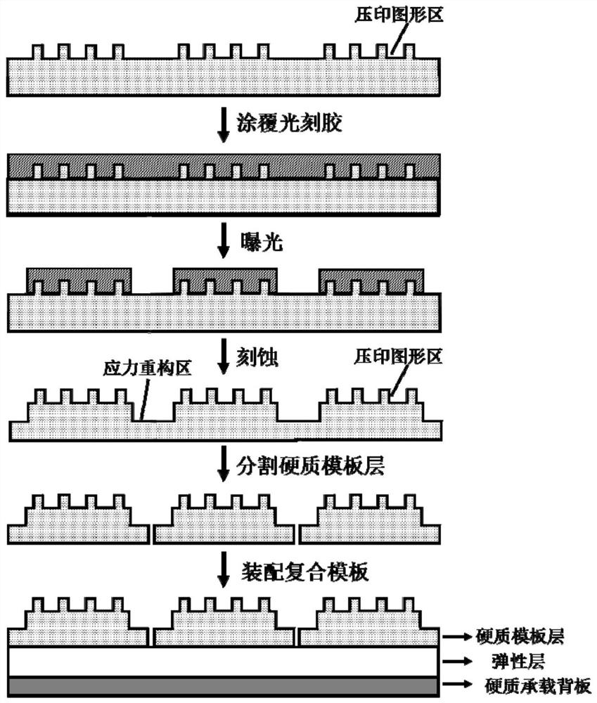
A kind of nano-imprint template and its preparation method and application
A nano-imprinting and template technology, which is applied in the field of nanotechnology, can solve the problems of low imprinting success rate and poor uniformity of stress distribution in the micro-area of the imprinting template, so as to improve the yield of imprinting and improve the uniformity of stress distribution in the micro-area , The effect of broadening the scope of the application structure
- Summary
- Abstract
- Description
- Claims
- Application Information
AI Technical Summary
Problems solved by technology
Method used
Image
Examples
Embodiment 1
[0085] The present embodiment provides a nano-imprint template, a preparation method thereof, and a nano-imprint method, which are as follows:
[0086] (1) Coating an adhesion promoter with a thickness of 10 nm on the silicon substrate, and then spin-coating a negative electron beam resist with a thickness of 350 nm, using a beam spot diameter of 5 nm and a dose of 300 μC / cm 2 The electron beam resist was exposed, developed and fixed with tetramethylammonium hydroxide solution and water, respectively, the samples were blown dry with nitrogen, and the samples were baked at 85 °C for 1 min.
[0087] (2) Oxygen plasma enhanced reactive ion etching was used to remove the electron beam resist pattern primer, and the etching time was 20s. Then use the negative electron beam resist pattern as a mask to etch the silicon substrate: the temperature of the stage is set to -110 ° C, and the gas SF is introduced. 6 and O 2 , the flow rate is 30sccm and 20sccm respectively, the power of t...
Embodiment 2
[0092] The present embodiment provides a nano-imprint template, a preparation method thereof, and a nano-imprint method, which are as follows:
[0093] (1) A positive electron beam resist with a thickness of 170 nm was spin-coated on a silicon substrate, using a beam spot diameter of 5 nm and a dose of 1000 μC / cm 2 The electron beam resist was exposed, developed and fixed to obtain a nanoarray pattern.
[0094] (2) A silicon oxide film with a thickness of 50 nm was evaporated on the electron beam resist pattern by the electron beam evaporation process, and the deposition rate was Then, the silicon substrate is placed in an acetone solution to perform a lift-off process to obtain a silicon oxide thin film pattern opposite to the exposure pattern.
[0095] (3) Using the silicon oxide film as a mask, the silicon substrate is etched: the temperature of the stage is set to -110°C, and the gas SF is introduced. 6 and O 2 , the flow rate is 30sccm and 12sccm, the power of the lower...
Embodiment 3
[0100] The present embodiment provides a nano-imprint template, a preparation method thereof, and a nano-imprint method, which are as follows:
[0101] (1) A positive electron beam resist with a thickness of 170 nm was spin-coated on a silicon substrate, using a beam spot diameter of 5 nm and a dose of 250 μC / cm 2 The electron beam resist was exposed, and the exposure pattern was the inverse pattern of Examples 1 and 2, and the nanoarray pattern was obtained after developing and fixing.
[0102] (2) Using the positive electron beam resist pattern as a mask, the silicon substrate is etched: the temperature of the stage is set to -110°C, and the gas SF is introduced. 6 and O 2 , the flow rate is 30s ccm and 15sccm, the lower electrode power is 5W, and the etching time is 35s. The e-beam resist is removed to obtain a silicon template structure (such as Figure 7a shown).
[0103] (3) Using optical exposure and dry etching technology to prepare a through channel structure of s...
PUM
| Property | Measurement | Unit |
|---|---|---|
| width | aaaaa | aaaaa |
Abstract
Description
Claims
Application Information


