An organic electroluminescent device, a preparation method thereof, and a display device prepared therefrom

An electroluminescent device and luminescence technology, which is applied in the manufacture of organic semiconductor devices, electric solid devices, semiconductor/solid state devices, etc., can solve problems such as black spots on devices, achieve good devices, reduce the influence of deformation, and have good application effects Effect

Active Publication Date: 2022-07-29
JIANGSU SUNERA TECH CO LTD
View PDF6 Cites 0 Cited by
  • Summary
  • Abstract
  • Description
  • Claims
  • Application Information

AI Technical Summary

Problems solved by technology

However, when making flexible devices, it is necessary to add a protective layer between the cover layer and the flexible packaging layer. The common material in the industry is LiF. However, the use of LiF has its disadvantages. It is prepared under CVD conditions. During the preparation process, a large amount of high-energy plasma will be generated, and large energy and electrons will be released to the internal layer structure of the device, which may promote the interaction between the organic material of the covering layer and the LiF of the adjacent layer, thereby Causes black spots on the device, so it needs to focus on solving this problem

Method used


Image

  • An organic electroluminescent device, a preparation method thereof, and a display device prepared therefrom
  • An organic electroluminescent device, a preparation method thereof, and a display device prepared therefrom
  • An organic electroluminescent device, a preparation method thereof, and a display device prepared therefrom

Examples


preparation example Construction

[0090] Preparation method of organic electroluminescent device

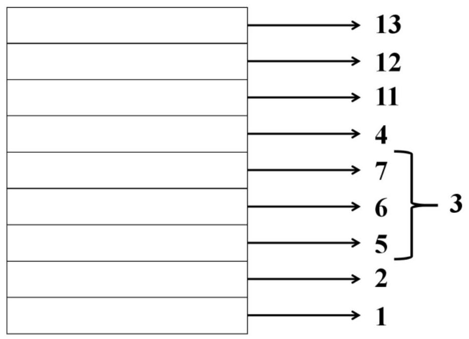
[0091] The present invention also relates to a method for preparing an organic electroluminescent device, which includes sequentially laminating a first electrode, an organic functional material layer and a second electrode on a substrate. Wherein, the organic functional material layer is formed by laminating a hole transport region, a light-emitting layer and an electron transport region successively from bottom to top on the first electrode, and the hole transport region is successively layered from bottom to top on the first electrode A hole injection layer, a hole transport layer and an electron blocking layer are formed, and the electron transport region is formed by sequentially laminating the electron transport layer and the electron injection layer on the light emitting layer from bottom to top.

[0092] Regarding the lamination, methods such as vapor deposition, vacuum evaporation, spin coating, castin...

Embodiment

[0102] Unless otherwise stated, various materials used in the following examples and comparative examples are commercially available or can be obtained by methods known to those skilled in the art. Table 3 Blue light organic electroluminescent devices prepared in Invention Examples 1-8 and Comparative Examples 1-2 and their properties.

[0103] table 3

[0104]

[0105] Description: Use the IVL (current-voltage-brightness) test system (Suzhou Fushida Scientific Instrument Co., Ltd.) to test, and the current density during the test is 10mA / cm 2 ; "-" means that the corresponding data cannot be tested, and the default is that the current efficiency is 0.

[0106] It can be seen from the results in Table 3 that compared with the use of active metal fluoride LiF, the current efficiency of the devices prepared in the device preparation examples 1-8 of the present invention is significantly improved, and the organic electroluminescence device of the present invention does not pr...


PUM

PropertyMeasurementUnit
thicknessaaaaaaaaaa
refractive indexaaaaaaaaaa

Abstract

The invention discloses an organic electroluminescence device, which comprises a substrate, a display unit, a cover layer, a protection layer and an encapsulation layer in order from bottom to top, and is characterized in that the cover layer contains a refractive index ≥ 1.8 and an absolute value of LUMO. Organic material ≥2.9 eV; the protective layer comprises one or more of cesium fluoroaluminate, magnesium fluoride, aluminum fluoride, and silver fluoride. The organic electroluminescent device of the invention overcomes the problem in the industry that the organic material of the cover layer interacts with the LiF of the adjacent layer due to TFE encapsulation, thereby causing the device to appear black spots, so that the yield is greatly improved and the production cost is reduced.

Description

technical field [0001] The present invention relates to the technical field of semiconductors, and in particular, to an organic electroluminescence device, a preparation method thereof, and a display device including the organic electroluminescence device. Background technique [0002] In recent years, organic electroluminescent diodes (OLEDs) have been researched and developed and widely used in display devices. As a current device, when a voltage is applied to the electrodes at both ends of the organic electroluminescence device, and the electric field acts on the positive and negative charges in the organic layer functional material film layer, the positive and negative charges are further recombined in the organic light-emitting layer, that is, a Electroluminescence. [0003] Currently, various methods that can improve light efficiency by efficiently extracting light generated in an organic light-emitting layer are urgently needed. An important method to realize the im...

Claims


Application Information

Patent Timeline
Patent Type & Authority Patents(China)
IPC IPC(8): H01L51/52H01L51/54H01L51/56
CPCH10K50/844H10K50/858H10K71/00H10K2102/00
Inventor 陈海峰李崇叶中华张兆超
Owner JIANGSU SUNERA TECH CO LTD
Why Eureka
Try Eureka