Preparation method of diamond with optical antireflection film

An optical anti-reflection coating and diamond technology, applied in optics, optical components, gaseous chemical plating, etc., can solve problems such as difficulties, achieve the effects of improving optical performance, optimizing product quality, and reducing production costs

Active Publication Date: 2021-02-19
UNIV OF SCI & TECH BEIJING +1
View PDF7 Cites 6 Cited by
  • Summary
  • Abstract
  • Description
  • Claims
  • Application Information

AI Technical Summary

Problems solved by technology

For such an extremely small diamond window material, it will obviously become very difficult to adopt the above-mentioned traditional anti-reflection coating method

Method used


Image

  • Preparation method of diamond with optical antireflection film
  • Preparation method of diamond with optical antireflection film
  • Preparation method of diamond with optical antireflection film

Examples


Embodiment 1

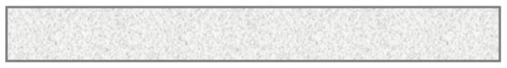
[0039]1) Single crystal silicon is used as the original substrate, the size of the original substrate is 10×10mm, and the thickness is 1mm. First, the substrate was cleaned, ultrasonically cleaned with acetone for 5 minutes, then transferred to alcohol for 10 minutes, and then dried with a hair dryer for later use, such as Figure 1a shown;

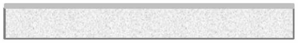
[0040] 2) The anti-reflection coating is plated by radio frequency sputtering. According to the short-wave infrared (wavelength 800-1500nm) anti-reflection requirements, the anti-reflection coating chooses Si 3 N 4 Material, the target film thickness is 125nm;

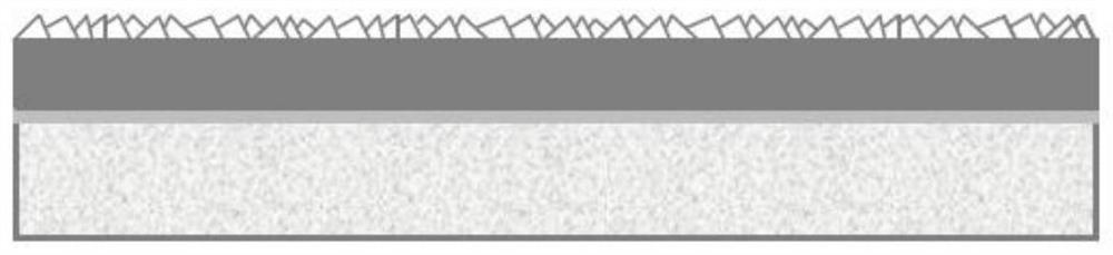
[0041] 3) After the original substrate is placed in the sputtering equipment, it is first vacuumed to 9×10 -4 Below Pa, heat the deposition table again, the heating temperature is 100°C, when it is heated to the corresponding temperature, the RF power supply voltage is 400V to remove oxygen; then the bias voltage: -800V, duty cycle: 30%, frequency: 45H Z Clean the substrate fo...

Embodiment 2

[0050] 1) Single crystal silicon is used as the original substrate, the size of the original substrate is 10×10mm, and the thickness is 1mm. First, the substrate was cleaned, ultrasonically cleaned with acetone for 5 minutes, then transferred to alcohol for 10 minutes, and then dried with a hair dryer for later use, such as Figure 1a shown;

[0051] 2) The anti-reflection coating is plated by radio frequency sputtering. According to the short-wave infrared (wavelength 800-1500nm) anti-reflection requirements, the anti-reflection coating chooses SiO 2 Material, the target film thickness is 160nm;

[0052] 3) After the original substrate is placed in the magnetron sputtering equipment, it is first vacuumed to 9×10 -4 Below Pa, heat the deposition table again, the heating temperature is 100°C, when the heating reaches the corresponding temperature, the RF power supply voltage is 400V for oxygen removal treatment; then bias voltage: -800V, duty cycle: 30%, frequency: 45H Z Cle...

Embodiment 3

[0061] 1) Metal Mo is used as the original substrate, the size of the original substrate is 10×10mm, and the thickness is 2mm. Firstly, polish the original substrate until the roughness is lower than 2nm; then clean it, use acetone to ultrasonically clean it for 5 minutes, then transfer it to alcohol for 10 minutes, and then dry it with a hair dryer for later use, such as Figure 1a shown;

[0062] 2) The anti-reflection coating is plated by magnetron sputtering. According to the anti-reflection requirements of long-wave infrared (wavelength 8-12μm), the anti-reflection coating is Y 2 o 3 Material, the target film thickness is 1100nm;

[0063] 3) After the original substrate is placed in the magnetron sputtering equipment, it is first vacuumed to 9×10 -4 Below Pa, heat the deposition table again, the heating temperature is 100°C, when heated to the corresponding temperature, the power supply voltage is 400V for oxygen removal treatment; then bias voltage: -800V, duty cycle:...


PUM

PropertyMeasurementUnit
surface roughnessaaaaaaaaaa

Abstract

The invention relates to a preparation method of diamond with an optical antireflection film, and particularly provides a self-supporting diamond material with an antireflection film and a preparationmethod thereof. The material can be used for windows of devices such as optical communication and sensors, and belongs to the field of optical material preparation and processing. The preparation method of the diamond with the optical antireflection film comprises the following steps of firstly, depositing the antireflection film on a polished original substrate; then preparing the diamond on thesurface of the antireflection film through chemical vapor deposition (CVD); carrying out grinding, polishing and laser scribing and cutting treatment on the surface of the prepared diamond; etching the surface of the processed diamond by adopting low-temperature plasma to remove a residual graphite phase on the surface; and removing the original substrate by adopting a chemical solution corrosionor ion selective etching mode, and reserving the diamond material with the antireflection film. The method is particularly suitable for meeting the application requirements of the fields of optical communication, micro sensors and the like on the micro diamond window material with the antireflection film.

Description

technical field [0001] The invention relates to a diamond preparation method with an optical anti-reflection film, in particular to a self-supporting diamond material with an anti-reflection film and a preparation method thereof. The material can be used in fields such as optical communication and sensor windows, and belongs to the field of optical material preparation and processing. Background technique [0002] In the fields of high-throughput optical communication and extreme environment detection, in order to protect high-precision signal processors from external environment erosion, it is generally necessary to set an optical window at the front end. The window material should have the characteristics of good optical transmission, high wear resistance, high chemical stability, etc., and the window must also have high heat transfer performance in extreme environments. The performance of traditional optical materials is difficult to meet all the above requirements at th...

Claims


Application Information

Patent Timeline
Patent Type & Authority Applications(China)
IPC IPC(8): C23C16/27C23C16/02C23C16/56C23C16/01G02B1/113
CPCC23C16/01C23C16/0272C23C16/27C23C16/56G02B1/113
Inventor 魏俊俊黄亚博陈良贤刘金龙李成明高旭辉
Owner UNIV OF SCI & TECH BEIJING
Why Eureka
Try Eureka