Anti-fuse memory cell and manufacturing method thereof

A technology of memory cells and manufacturing methods, applied in the field of semiconductors, capable of solving problems such as damage to select gate structures

Pending Publication Date: 2021-02-23
CHANGXIN MEMORY TECH INC
View PDF0 Cites 2 Cited by
  • Summary
  • Abstract
  • Description
  • Claims
  • Application Information

AI Technical Summary

Problems solved by technology

[0005] Embodiments of the present invention provide an antifuse memory unit and a manufacturing method thereof, which solve the problem that the source/drain i

Method used


Image

  • Anti-fuse memory cell and manufacturing method thereof
  • Anti-fuse memory cell and manufacturing method thereof
  • Anti-fuse memory cell and manufacturing method thereof

Examples


Embodiment Construction

[0024] It can be seen from the background art that the selection gate dielectric layer in the antifuse memory cell in the prior art is prone to damage.

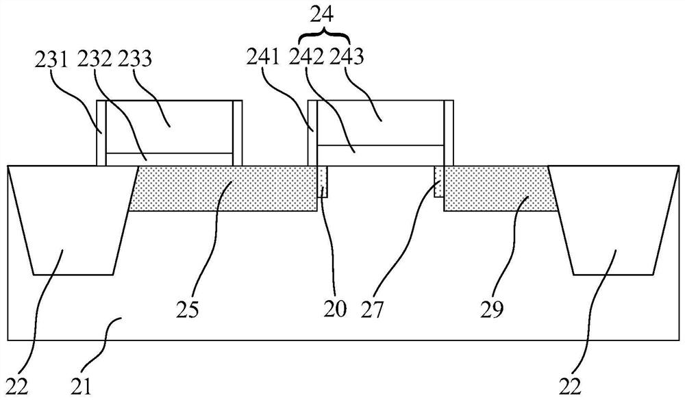
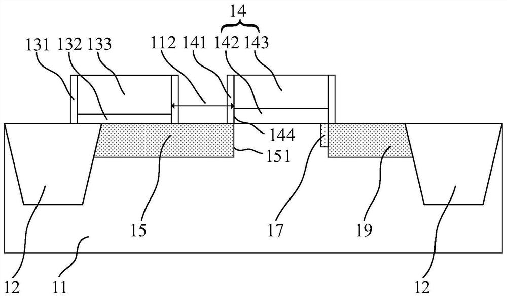
[0025] refer to figure 1 , figure 1 It is a schematic cross-sectional structure diagram of an antifuse memory cell. refer to figure 1 , the antifuse memory unit comprises: a substrate 21 with a select gate structure 24 on the substrate; a first doped region 25 and a second doped region 29, the first doped region 25 and the second doped region 29 respectively In the substrate 21 located on opposite sides of the select gate structure 24, the doping ion types of the first doped region 25 and the second doped region 29 are the same; the antifuse gate dielectric layer located on the first doped region 25 232 and the antifuse gate 233 located on the antifuse gate dielectric layer 232; the third doped region 27, the third doped region 27 is located between the second doped region 29 and the select gate structure 24, the third Th...


PUM


Abstract

The embodiment of the invention relates to an anti-fuse memory cell and a manufacturing method thereof, and the anti-fuse memory cell comprises a substrate which is provided with a selection gate structure, a first doped region and a second doped region, an anti-fuse gate dielectric layer, an anti-fuse gate, and a third doped region. The first doped region and the second doped region are respectively located in the substrate at two opposite sides of the selection gate structure, and the doped ion types of the first doped region and the second doped region are the same; the anti-fuse gate dielectric layer is positioned on the first doped region; the anti-fuse gate is positioned on the anti-fuse gate dielectric layer; and the third doped region is located between the second doped region andthe selection gate structure, the doped ion type of the third doped region is the same as that of the second doped region, and the doped ion concentration of the third doped region is smaller than that of the second doped region. Damage of an electric field to the selection gate dielectric layer can be reduced, so that the reliability of the selection transistor in the anti-fuse storage unit is improved.

Description

technical field [0001] The invention relates to the technical field of semiconductors, in particular to an antifuse memory unit and a manufacturing method thereof. Background technique [0002] Memory devices can generally be classified into volatile memory devices and non-volatile storage devices. Non-volatile storage devices can be further classified into read only memory (ROM), one time programmable memory (OTP memory) and re-readable memory. Among them, the one-time programmable memory can be classified into fuse type and anti-fuse type. [0003] In semiconductor devices such as DRAM (Dynamic Random Access Memory), generally redundant cells are used to replace defective cells that cannot work normally, so as to repair defective addresses. In storing defect addresses, antifuse memory is often used to store information. [0004] The smallest unit of an antifuse memory usually consists of an antifuse transistor and a select transistor. The working principle of the antif...

Claims


Application Information

Patent Timeline
IPC IPC(8): H01L27/112H01L21/8246G11C17/16
CPCG11C17/16H10B20/20
Inventor 冯鹏李雄
Owner CHANGXIN MEMORY TECH INC
Why Eureka
Try Eureka