Inverted organic light-emitting diode device and preparation method thereof

An electroluminescent device, an organic technology, applied in the direction of organic semiconductor devices, electric solid devices, semiconductor/solid device manufacturing, etc., can solve the problems of low efficiency and high driving voltage

Active Publication Date: 2021-02-23
SHANGHAI UNIV
View PDF4 Cites 0 Cited by
  • Summary
  • Abstract
  • Description
  • Claims
  • Application Information

AI Technical Summary

Problems solved by technology

However, OLED devices based on SnO2 as the electron injection layer still have problems such as high driving voltage and low efficiency.

Method used


Image

  • Inverted organic light-emitting diode device and preparation method thereof
  • Inverted organic light-emitting diode device and preparation method thereof
  • Inverted organic light-emitting diode device and preparation method thereof

Examples


Embodiment 1

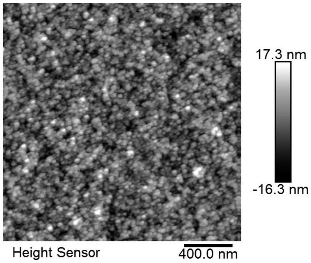
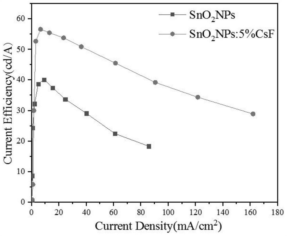
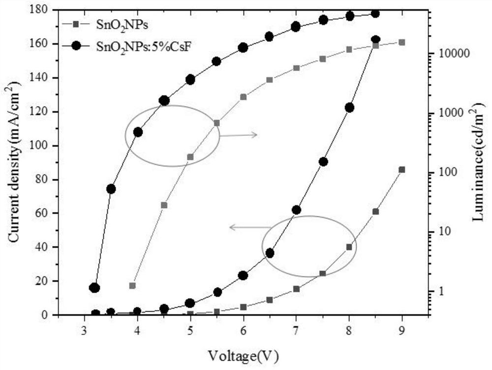
[0051] In this embodiment, an inverted organic electroluminescent device includes an ITO substrate, a doped electron injection layer, an energy level matching layer, a hole blocking layer, a light emitting layer, a hole transport layer, a hole injection layer and an anode layer; the doped electron injection layer is SnO doped with tin dioxide nanoparticles by cesium fluoride particles 2 : CsF composite material layer; in the doped electron injection layer, the doping mass percentages of the cesium fluoride particles are respectively 3%, 5% and 10%; the annealing temperature of the doped electron injection layer is 150 ° C; the thickness of the doped electron injection layer is 30 nm.

[0052] In this embodiment, the method for preparing an inverted organic electroluminescent device in this embodiment includes the following steps:

[0053] S1.ITO substrate pretreatment:

[0054] Clean and dry the ITO substrate to obtain the processed ITO substrate; the pretreatment process of...

Embodiment 2

[0071] This embodiment is basically the same as Embodiment 1, and the special features are:

[0072] In this embodiment, an inverted organic electroluminescent device includes an ITO substrate, a doped electron injection layer, an energy level matching layer, a hole blocking layer, a light emitting layer, a hole transport layer, a hole injection layer and an anode layer; the doped electron injection layer is SnO doped with tin dioxide nanoparticles by cesium fluoride particles 2 : CsF composite material layer; in the doped electron injection layer, the doping mass percentage of the cesium fluoride particles is 5%; the annealing temperature of the doped electron injection layer is respectively 120 ℃ and 180 ℃; the The thickness of the doped electron injection layer is 30nm.

[0073] In this embodiment, the method for preparing an inverted organic electroluminescent device in this embodiment includes the following steps:

[0074] S1.ITO substrate pretreatment:

[0075] Clean ...

Embodiment 3

[0100] This embodiment is basically the same as the previous embodiment, and the special features are:

[0101] In this embodiment, an inverted organic electroluminescent device includes an ITO substrate, a doped electron injection layer, an energy level matching layer, a hole blocking layer, a light emitting layer, a hole transport layer, a hole injection layer and an anode layer; the doped electron injection layer is SnO doped with tin dioxide nanoparticles by cesium fluoride particles 2 : CsF composite material layer; in the doped electron injection layer, the doping mass percentage of the cesium fluoride particles is 5%; the annealing temperature of the doped electron injection layer is respectively 150 ° C; the doped The thickness of the type electron injection layer was 25 nm.

[0102] In this embodiment, the method for preparing an inverted organic electroluminescent device in this embodiment includes the following steps:

[0103] S1.ITO substrate pretreatment:

[01...


PUM

PropertyMeasurementUnit
thicknessaaaaaaaaaa
thicknessaaaaaaaaaa
thicknessaaaaaaaaaa

Abstract

The invention discloses an inverted organic light-emitting diode device and a preparation method thereof. The performance of the inverted organic light-emitting diode device is improved by enhancing electron injection. The inverted organic light-emitting diode device structure comprises an ITO substrate, a doped electron injection layer, an energy level matching layer, a hole blocking layer, a light-emitting layer, a hole transport layer, a hole injection layer and an anode layer; according to the preparation method, a methanol solution of cesium fluoride is used for treating a stannic oxide solution through a solution process, and the electron mobility of the prepared cesium fluoride doped stannic oxide nanoparticle film is improved compared with that of an untreated stannic oxide film. The stannic oxide film is used as an electron injection layer of an inverted organic light-emitting diode device, so that compared with a device in which an untreated stannic oxide film is used as theelectron injection layer, the electronic current of the device is increased, and the driving voltage is reduced. The doped electron injection layer is prepared by a solution method with a simple process, and an effective scheme is provided for realizing inverted solution processing of an OLED device with low driving voltage and high efficiency.

Description

technical field [0001] The invention relates to the field of organic electroluminescence, in particular to an inverted organic electroluminescence device and a preparation method thereof. Background technique [0002] In recent years, organic electroluminescent devices (OLEDs) have been widely used in real life, especially in the fields of solid-state lighting and display. In order to meet the requirements of preparation, a variety of device manufacturing process technologies have gradually been developed, including wet processes represented by wet chemistry, spray pyrolysis, and spraying methods, and pulsed laser deposition, chemical vapor deposition, and thermal evaporation. The dry process is the most widely used. Generally speaking, the process development trend is gradually from complex to simple process. Due to the advantages of simple process, low cost, and large-area mass production, the wet process represented by the wet chemical method has attracted more and more...

Claims


Application Information

Patent Timeline
Patent Type & Authority Applications(China)
IPC IPC(8): H01L51/50H01L51/54H01L51/56
CPCH10K50/171H10K2102/102H10K2102/321H10K71/00Y02E10/549
Inventor 朱文清刘丹陈瑞琳万敏强张建华
Owner SHANGHAI UNIV
Why Eureka
Try Eureka