Flexible memory based on two-dimensional material

A two-dimensional material and memory technology, applied in the field of non-volatile memory, can solve problems such as gate application, achieve the effect of reducing energy consumption and realizing multi-functionality

Active Publication Date: 2021-03-02
BEIJING INSTITUTE OF TECHNOLOGYGY
View PDF6 Cites 2 Cited by
  • Summary
  • Abstract
  • Description
  • Claims
  • Application Information

AI Technical Summary

Problems solved by technology

However, in order to make this device reach the erased state, it is necessary to apply a large positive voltage to the gate, so high power consumption is inevitable for the device to work normally.

Method used


Image

  • Flexible memory based on two-dimensional material
  • Flexible memory based on two-dimensional material
  • Flexible memory based on two-dimensional material

Examples


Embodiment 1

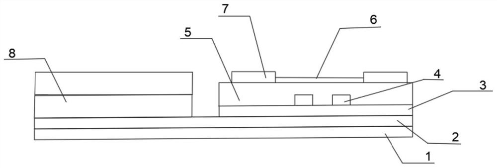
[0032] A flexible memory based on two-dimensional materials, including a flexible substrate, and an indium tin oxide layer, an aluminum oxide barrier layer, a nano-graphene layer, an aluminum oxide tunneling layer, and a di Molybdenum sulfide layer, metal electrode;

[0033] The preparation method of the flexible memory based on the two-dimensional material described in embodiment 1 comprises the following steps:

[0034] (1) Deposit indium tin oxide on a flexible substrate by magnetron sputtering to make an indium tin oxide layer with a thickness of 20nm as the bottom electrode;

[0035] (2) Aluminum oxide is deposited on the surface of the indium tin oxide layer as an aluminum oxide barrier layer by atomic layer deposition, and the thickness of the aluminum oxide barrier layer is 20nm;

[0036] (3) Graphene is deposited on the silicon chip that is covered with silicon oxide by the method for plasma chemical vapor deposition, and the silicon chip is covered with the thicknes...

Embodiment 2

[0042] A flexible memory based on two-dimensional materials, including a flexible substrate, and an indium tin oxide layer, an aluminum oxide barrier layer, a nano-graphene layer, an aluminum oxide tunneling layer, and a di Molybdenum sulfide layer, metal electrode;

[0043] The preparation method of the flexible memory based on the two-dimensional material described in embodiment 2 comprises the following steps:

[0044](1) Deposit indium tin oxide on a flexible substrate by magnetron sputtering to make an indium tin oxide layer with a thickness of 30nm as the bottom electrode;

[0045] (2) Aluminum oxide is deposited on the surface of the indium tin oxide layer as an aluminum oxide barrier layer by atomic layer deposition, and the thickness of the aluminum oxide barrier layer is 30nm;

[0046] (3) Graphene is deposited on the silicon chip that is covered with silicon oxide by the method for plasma chemical vapor deposition, and the silicon chip is covered with the thickness...

Embodiment 3

[0052] A flexible memory based on two-dimensional materials, including a flexible substrate, and an indium tin oxide layer, an aluminum oxide barrier layer, a nano-graphene layer, an aluminum oxide tunneling layer, and a di Molybdenum sulfide layer, metal electrode;

[0053] The preparation method of the flexible memory based on the two-dimensional material described in embodiment 3 comprises the following steps:

[0054] (1) Deposit indium tin oxide on a flexible substrate by magnetron sputtering to make an indium tin oxide layer with a thickness of 50 nm as the bottom electrode;

[0055] (2) Aluminum oxide is deposited on the surface of the indium tin oxide layer as an aluminum oxide barrier layer by atomic layer deposition, and the thickness of the aluminum oxide barrier layer is 25nm;

[0056] (3) Graphene is deposited on a silicon wafer covered with silicon oxide by plasma chemical vapor deposition, and the silicon wafer is covered with a thickness of 320nm of silicon ox...


PUM

PropertyMeasurementUnit
thicknessaaaaaaaaaa
thicknessaaaaaaaaaa
thicknessaaaaaaaaaa

Abstract

The invention discloses a flexible memory based on a two-dimensional material. The flexible memory comprises a flexible substrate, and an indium tin oxide layer, an aluminum oxide barrier layer, a nano graphene layer, an aluminum oxide tunneling layer, a molybdenum disulfide layer and a metal electrode which are sequentially arranged on the flexible substrate from bottom to top. The flexible memory based on the two-dimensional material has the beneficial effects that the flexible memory utilizes the density-adjustable nano graphene to effectively capture, release and transfer electrons under different working conditions, so that the writing and erasing processes of a device are realized; and the multi-state storage performance of the flexible memory under the action of different mechanicaland optical signals is realized by utilizing the combined action of the input voltage provided by a nano-generator under mechanical motion and incident illumination.

Description

technical field [0001] The invention relates to the field of non-volatile memory, in particular to a flexible memory based on two-dimensional materials. Background technique [0002] In recent years, considering the new requirements for device miniaturization and structural flexibility, two-dimensional materials have achieved rapid development in the research of flexible memories due to their excellent electrical and mechanical properties, which can achieve larger storage windows, lower The working voltage and better data retention characteristics. Although the performance of memory based on two-dimensional materials cannot be compared with that of silicon-based memory at this stage, its high storage density, fast erasing performance, and adaptability to various complex environments are important supplements to the non-volatile semiconductor memory market. . However, in order to realize its commercial practical application, the following problems need to be solved: (1) Imp...

Claims


Application Information

Patent Timeline
Patent Type & Authority Applications(China)
IPC IPC(8): H01L27/11521B81B7/02B82Y40/00
CPCB81B7/02B82Y40/00H10B41/30
Inventor 赵静
Owner BEIJING INSTITUTE OF TECHNOLOGYGY
Why Eureka
Try Eureka