Memory and forming method thereof

A memory and graphics technology, applied in the manufacture of electric solid-state devices, semiconductor devices, semiconductor/solid-state devices, etc., can solve the problem of high dielectric constant, affecting signal transmission speed and strength, coupling effect of metal bit lines and capacitive contact lines, etc. problem, achieve the effect of small dielectric constant, improve isolation performance, and reduce parasitic capacitance

Active Publication Date: 2021-03-05
CHANGXIN MEMORY TECH INC
View PDF9 Cites 6 Cited by
  • Summary
  • Abstract
  • Description
  • Claims
  • Application Information

AI Technical Summary

Problems solved by technology

Usually the insulating material between the bit line and the capacitor contact line is silicon nitride, and the dielectric constant of silicon nitride is relatively high (close to 8), which will cause a serious coupling effect between the metal bit line and the capacitor contact line , affecting the transmission speed and strength of the signal, therefore, the performance of the existing memory needs to be further improved

Method used


Image

  • Memory and forming method thereof
  • Memory and forming method thereof
  • Memory and forming method thereof

Examples


Embodiment Construction

[0024] The specific implementation of the memory provided by the present invention and its forming method will be described in detail below in conjunction with the accompanying drawings.

[0025] Please refer to Figure 1A to Figure 12 It is a structural schematic diagram of the forming process of the memory according to a specific embodiment of the present invention.

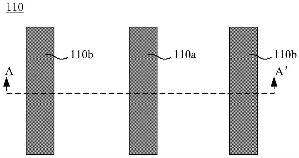
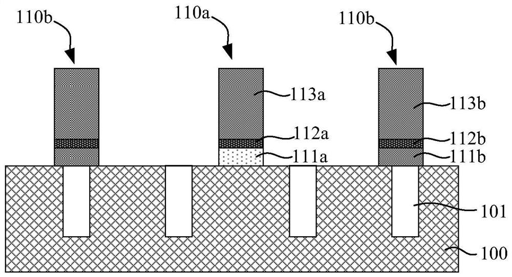
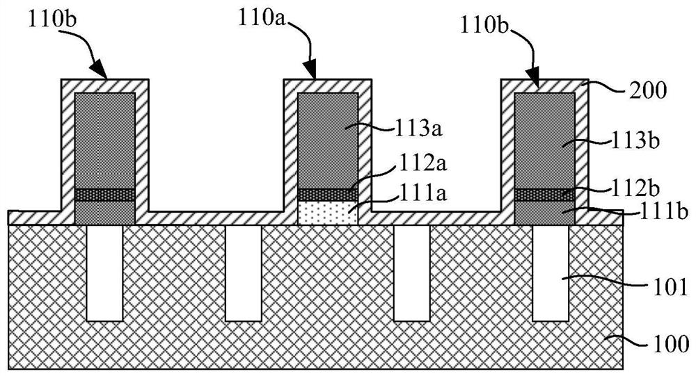
[0026] Please refer to Figure 1A and 1B 1. A substrate 100 is provided, and a plurality of bit line structures 110 arranged at intervals are formed on the substrate 100 . 1A is a schematic top view of the bit line structure 110 . Figure 1B for along Figure 1A Schematic cross-sectional view of the secant line AA'.

[0027] The semiconductor substrate 100 may include but not limited to a single crystal silicon substrate, a polycrystalline silicon substrate, a gallium nitride substrate or a sapphire substrate. In addition, when the semiconductor substrate 100 is a single crystal substrate or a polycrystalli...


PUM

PropertyMeasurementUnit
Thicknessaaaaaaaaaa

Abstract

The invention discloses a memory and a forming method thereof. The forming method of the memory comprises the steps: providing a substrate, and forming a plurality of bit line structures which are arranged at intervals on the substrate; forming a covering layer at least covering the side walls of the bit line structures; forming filling layers on the substrate, wherein gaps between adjacent bit line structures are filled with the filling layers; etching the filling layers to the surface of the substrate to form contact holes, wherein the filling layers with partial thickness are arranged between the contact holes and the covering layer; forming a conductive plug in each contact hole; removing the remaining filling layers; and filling an insulating layer on the substrate, sealing a space between the covering layer and the conductive plug by the insulating layer, and forming an air gap between the covering layer and the conductive plug. The performance of the memory is improved.

Description

technical field [0001] The invention relates to the technical field of semiconductors, in particular to a memory and a forming method thereof. Background technique [0002] The development of memory pursues high speed, high integration density, low power consumption and so on. With the shrinking of the structure size of semiconductor devices, especially in the manufacturing process of DRAM with critical dimensions less than 20nm, there are higher requirements for insulating materials between wires, such as wider bandwidth to ensure good insulation performance, lower The dielectric constant is used to ensure small parasitic capacitance and small coupling effect. Various low-k dielectric materials are widely used in semiconductor manufacturing. Among them, the air layer structure of silicon nitride-air layer-silicon nitride is one of the optimal low-K dielectric material structures. Since the air layer in the middle can ensure its good insulation performance, and the air laye...

Claims


Application Information

Patent Timeline
IPC IPC(8): H01L21/8242H01L21/768H01L27/108
CPCH01L21/7682H10B12/31H10B12/0335H10B12/482
Inventor 陈龙阳吴公一
Owner CHANGXIN MEMORY TECH INC
Why Eureka
Try Eureka