DRAM and forming method thereof

A memory and wet etching technology, applied in the field of memory, can solve problems such as limited number and limited DRAM integration

Pending Publication Date: 2021-03-05
CHANGXIN MEMORY TECH INC
View PDF0 Cites 1 Cited by
  • Summary
  • Abstract
  • Description
  • Claims
  • Application Information

AI Technical Summary

Problems solved by technology

[0004] Due to the constraints of word line resistance and capacitance-related factors, the number of transistors contained in a single chip of an existing DRAM is limited (generally 1024), which greatly limits the integration of DRAM, so how to reduce word line resistance and improve storage The conduction current of the unit transistor has become a key and difficult problem in the development of DRAM, which needs to be solved urgently

Method used


Image

  • DRAM and forming method thereof
  • DRAM and forming method thereof
  • DRAM and forming method thereof

Examples


Embodiment Construction

[0034] As mentioned in the background art, how to reduce the word line resistance and increase the conduction current of the memory cell transistor has become a key and difficult problem in the development of DRAM, which needs to be solved urgently.

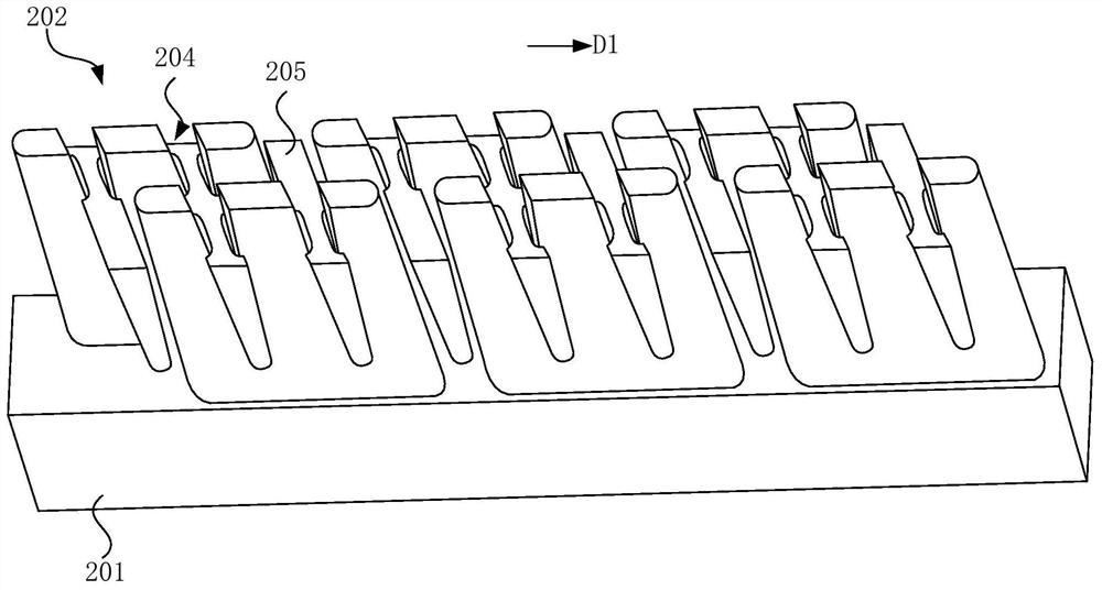
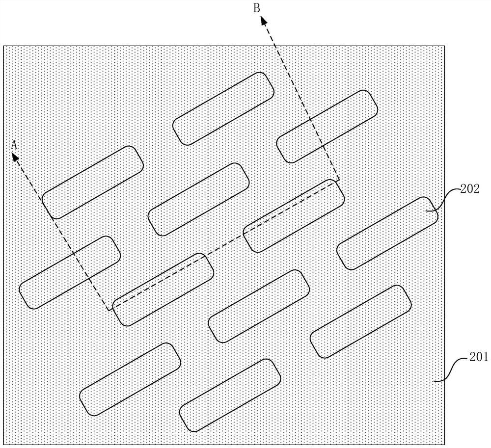
[0035] The study found that compared with the linear gate (or word line structure) formed in the existing semiconductor substrate, the effective cross-sectional area of ​​the wavy word line will be larger, which will effectively reduce the resistance of the word line, making the word line drive It can be quickly driven from a low potential to a high potential, improving the operation speed of the DRAM memory.

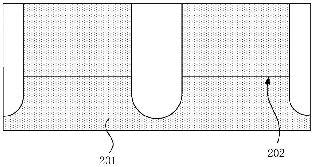
[0036] For this reason, the present invention provides a kind of DRAM memory and its forming method, described forming method, after etching described active region and isolation layer to form word line groove, along the sidewall of word line groove in described isolation layer Continue etching the isolation layer to widen...


PUM

PropertyMeasurementUnit
Widthaaaaaaaaaa

Abstract

The invention discloses a DRAM and a forming method thereof. The method comprises the following steps: after the active region and the isolation layer are etched to form a word line trench, continuously etching the isolation layer along the side wall of the word line trench in the isolation layer, so that the width of the word line trench in the isolation layer is increased, and the width of the part of the word line trench in the isolation layer is greater than that of the part of the word line trench in the active region; and forming a word line structure in the word line trench, wherein thewidth of the part of word line structure in the isolation layer is greater than the width of the part of word line structure in the active region. The formed word line structure is wavy, so that on one hand, the resistance of the word line structure is reduced; and on the other hand, a channel is formed at the boundary of the active region, that is, the width of the conductive channel of a deviceis increased, and the conduction current of the transistor of the DRAM is increased, so that the reading speed of memory is increased, and the integration level of the transistor of the DRAM is increased.

Description

technical field [0001] The invention relates to the field of memory, in particular to a DRAM memory and a forming method thereof. Background technique [0002] Dynamic Random Access Memory (Dynamic Random Access Memory, DRAM) is a semiconductor storage device commonly used in computers, and is composed of many repeated storage units. Each memory cell usually includes a capacitor and a transistor. The gate of the transistor is connected to the word line, the drain is connected to the bit line, and the source is connected to the capacitor. The voltage signal on the word line can control the opening or closing of the transistor, and then through the bit line Read the data information stored in the capacitor, or write the data information into the capacitor through the bit line for storage. [0003] In order to improve the integration of the storage structure, the transistors in the DRAM memory usually adopt a trench-shaped transistor structure. The specific structure of the tr...

Claims


Application Information

Patent Timeline
IPC IPC(8): H01L21/8242H01L27/108H01L21/311
CPCH01L21/31111H01L21/31144H10B12/30H10B12/488
Inventor 李宁
Owner CHANGXIN MEMORY TECH INC
Why Eureka
Try Eureka